DE0-Nano Interface Board Connections: Difference between revisions
Ghalfacree (talk | contribs) (Added pin-out table.) |
AndrewBack (talk | contribs) No edit summary |
||
| (One intermediate revision by one other user not shown) | |||
| Line 149: | Line 149: | ||
====JA1 - FPGA Module Connectors Array==== | ====JA1 - FPGA Module Connectors Array==== | ||
JA1 is a connection array for the DEO-Nano FPGA Development System. Physically, there are two separate connectors on the board. This connector establishes the interface between the Myriad-RF 1 board's digital interface and FPGA module with the PC. | JA1 is a connection array for the DEO-Nano FPGA Development System. Physically, there are two separate connectors on the board. This connector establishes the interface between the Myriad-RF 1 board's digital interface and FPGA module with the PC. | ||
[[File:DE0-Nano-JA1.jpg| | [[File:DE0-Nano-JA1.jpg|center|550px|DE0-Nano Interface Board JA1]] | ||
{| class="wikitable" | {| class="wikitable" | ||
! scope="row" colspan="6" | JA1 GPIO_0 | ! scope="row" colspan="6" | JA1 GPIO_0 | ||
| Line 295: | Line 295: | ||
* [[RFDIO|RFDIO Interface]] | * [[RFDIO|RFDIO Interface]] | ||
* [https://myriadrf.org/projects/rdk/ Reference Development Kit Project Page] | * [https://myriadrf.org/projects/rdk/ Reference Development Kit Project Page] | ||
{{Community}} | |||
Latest revision as of 15:04, 15 September 2015
DE0-Nano Interface Board Connections
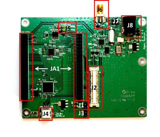
The following table describes the pin assignment for each connector on the digital interface board:
| Connector | Name | Description |
|---|---|---|
| J1 | RF PWR | Optional +5 V power supply for the Myriad-RF 1 board. |
| J2 | Digital I/O | The FX10A-80P is a standard connector used to interface the Myriad-RF board directly to a base band board. |
| J3 | FPGA PWR | Optional +5 V power supply for the FPGA module. |
| J4 | Mini-USB | Port used to connect to USB microcontroller. |
| J5 | EEPROM Boot | Enables memory access for USB microcontroller. |
| J6 | CLK Output | Used to synchronise measurement equipment. Clock output is generated with onboard frequency synthesiser. |
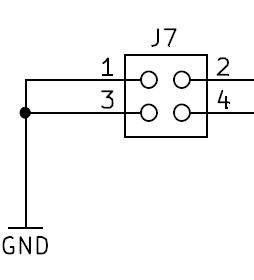
| J7 | Frequency Synthesiser Enable | Programmable synthesiser operation control. Enables synthesiser outputs. |
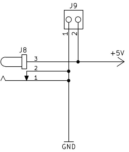
| J8 | Main Power Supply | +5 V power supply feed for digital interface board as well as Myriad-RF 1 board. Connector type SPC4077. |
| J9 | Main Power Supply | +5 V power supply feed for digital interface board as well as Myriad-RF 1 board. Connector type two-way pin header. |
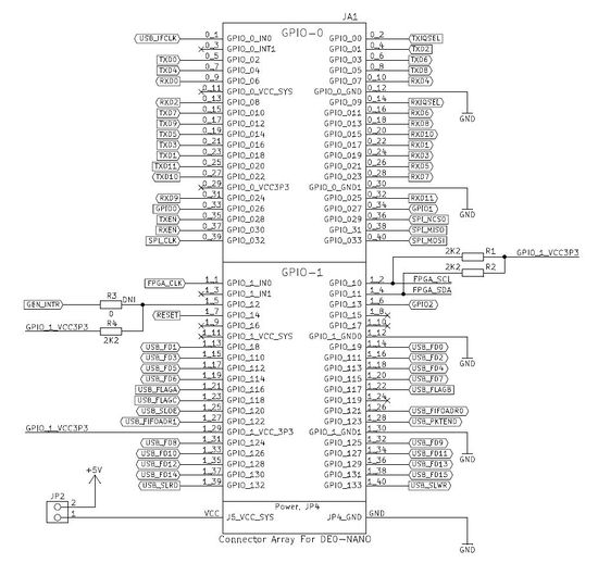
| JA1 | FPGA Module Connectors Array | The connector array designed to plug a DE0-Nano FPGA Development System onto the interface board. |
J1 and J3 - +5 V Power Connectors
These pin header type connectors used as jumpers to supply +5 V for the Myriad-RF 1 board and DE0-Nano FPGA module. The options are used as shown below:
- Use jumper on J1 if Myriad-RF 1 is to receive power from the interface board.
- Use jumper on J3 if DE0-Nano power is supplied from the interface board.
J2 - Digital I/O Connector
The Myriad-RF board is directly plugged into the J2 connector. The digital I/O connector is a digital transmit (TX) and receive (RX) interface to the ADC/DAC of the LMS6002D. The SPI interface for LMS6002DFN can also be established via J2 connector.
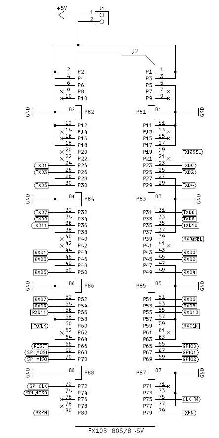
| Pin Nr | Function | Description | Pin Nr | Function | Description |
|---|---|---|---|---|---|
| 1 | 5V | Power | 2 | 5V | Power |
| 3 | 5V | Power | 4 | 5V | Power |
| 5 | GND | Power | 6 | GND | Power |
| 7 | NC | No connection | 8 | NC | No connection |
| 9 | NC | No connection | 10 | NC | No connection |
| 81 | GND | Power | 82 | GND | Power |
| 11 | GND | Power | 12 | GND | Power |
| 13 | NC | No connection | 14 | NC | No connection |
| 15 | NC | No connection | 16 | NC | No connection |
| 17 | GND | Power | 18 | GND | Power |
| 19 | TXIQSEL | CMOS Out | 20 | NC | No connection |
| 21 | NC | No connection | 22 | NC | No connection |
| 23 | TXD0 | CMOS IO | 24 | TXD1 | CMOS IO |
| 25 | TXD2 | CMOS IO | 26 | TXD3 | CMOS IO |
| 27 | GND | Power | 28 | GND | Power |
| 29 | TXD4 | CMOS IO | 30 | TXD5 | CMOS IO |
| 83 | GND | Power | 84 | GND | Power |
| 31 | TXD6 | CMOS IO | 32 | TXD7 | CMOS IO |
| 33 | TXD8 | CMOS IO | 34 | TXD9 | CMOS IO |
| 35 | TXD10 | CMOS IO | 36 | TXD11 | CMOS IO |
| 37 | GND | Power | 38 | GND | Power |
| 39 | RXIQSEL | CMOS In | 40 | NC | No connection |
| 41 | NC | No connection | 42 | NC | No connection |
| 43 | RXD0 | CMOS IO | 44 | RXD1 | CMOS IO |
| 45 | RXD2 | CMOS IO | 46 | RXD3 | CMOS IO |
| 47 | GND | Power | 48 | GND | Power |
| 49 | RXD4 | CMOS IO | 50 | RXD5 | CMOS IO |
| 85 | GND | Power | 86 | GND | Power |
| 51 | RXD6 | CMOS IO | 52 | RXD7 | CMOS IO |
| 53 | RXD8 | CMOS IO | 54 | RXD9 | CMOS IO |
| 55 | RXD10 | CMOS IO | 56 | RXD11 | CMOS IO |
| 57 | GND | Power | 58 | GND | Power |
| 59 | RXCLK | Receive Clock | 60 | TXCLK | Transmit Clock |
| 61 | NC | No connection | 62 | NC | No connection |
| 63 | GND | Power | 64 | GND | Power |
| 65 | GPIO0 | CMOS In | 66 | RESET | CMOS In |
| 67 | GPIO1 | CMOS In | 68 | SPI_MOSI | CMOS In |
| 69 | GPIO2 | CMOS In | 70 | SPI_MISO | CMOS Out |
| 87 | GND | Power | 88 | GND | Power |
| 71 | NC | No Connection | 72 | SPI_CLK | CMOS In |
| 73 | GND | Power | 74 | SPI_NCS0 | CMOS In |
| 75 | CLK_IN | CMOS reference CLK input for RF Card | 76 | NC | No connection |
| 77 | GND | Power | 78 | NC | No connection |
| 79 | TXEN | CMOS In | 80 | RXEN | CMOS In |
J4 - Mini-USB Connector
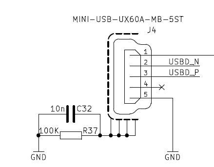
The interface with USB microcontroller and PC is established via mini USB connector. This connector also powers the microcontroller.
J5 - EEPROM Boot Memory Connector
This connector enables the USB microcontroller to load the firmware at startup.
J6 - CLK Output Connector
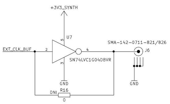
J6 is an SMA type connector, used to synchronise measurement equipment with the development kit.
J7 - Frequency Synthesiser Enable Connector
J7 is a pin-header type connector. Pin 3 and Pin 4 have to be shorted in normal operation, thus enabling frequency synthesiser outputs.
J8 and J9 - Main Power Supply Connectors
The main power supply connector is on the interace board, providing power to both the interface as well as the Myriad-RF 1 board.
JA1 - FPGA Module Connectors Array
JA1 is a connection array for the DEO-Nano FPGA Development System. Physically, there are two separate connectors on the board. This connector establishes the interface between the Myriad-RF 1 board's digital interface and FPGA module with the PC.
| JA1 GPIO_0 | |||||
|---|---|---|---|---|---|
| Pin Nr | Function | Description | Pin Nr | Function | Description |
| 1 | USB_IFCLK | USB interface clock | 2 | TXIQSEL | CMOS in |
| 3 | NC | No connection | 4 | TXD2 | CMOS IO |
| 5 | TXD0 | CMOS IO | 6 | TXD6 | CMOS IO |
| 7 | TXD4 | CMOS IO | 8 | TXD8 | CMOS IO |
| 9 | RXD0 | CMOS IO | 10 | RXD4 | CMOS IO |
| 11 | VCC_SYS | Power | 12 | GND | Power |
| 13 | RXD2 | CMOS IO | 14 | RXIQSEL | CMOS in |
| 15 | TXD7 | CMOS IO | 16 | RXD6 | CMOS IO |
| 17 | TXD9 | CMOS IO | 18 | RXD8 | CMOS IO |
| 19 | TXD5 | CMOS IO | 20 | RXD10 | CMOS IO |
| 21 | TXD3 | CMOS IO | 22 | RXD1 | CMOS IO |
| 23 | TXD1 | CMOS IO | 24 | RXD3 | CMOS IO |
| 25 | TXD11 | CMOS IO | 26 | RXD5 | CMOS IO |
| 27 | TXD10 | CMOS IO | 28 | RXD7 | CMOS IO |
| 29 | VCC3P3 | Power | 30 | GND | Power |
| 31 | RXD9 | CMOS IO | 32 | RXD11 | CMOS IO |
| 33 | GPIO0 | CMOS IO | 34 | GPIO1 | CMOS IO |
| 35 | TXEN | CMOS in | 36 | SPI_NCS0 | CMOS in |
| 37 | RXEN | CMOS in | 38 | SPI_MISO | CMOS out |
| 39 | SPI_CLK | CMOS in | 40 | SPI_MOSI | CMOS in |
| JA1 GPIO_1 | |||||
| Pin Nr | Function | Description | Pin Nr | Function | Description |
| 1 | FPGA_CLK | FPGA clock | 2 | FPGA_SCL | FPGA in |
| 3 | NC | No connection | 4 | FPGA_SDA | FPGA IO |
| 5 | GEN_INTR | Via R3 and R4 to GPIO_1_VCC3P3 | 6 | GPIO2 | CMOS IO |
| 7 | RESET | Reset line | 8 | NC | No connection |
| 9 | NC | No connection | 10 | NC | No connection |
| 11 | VCC_SYS | Power | 12 | GND | Power |
| 13 | USB_FD1 | USB | 14 | USB_FD0 | USB |
| 15 | USB_FD3 | USB | 16 | USB_FD2 | USB |
| 17 | USB_FD5 | USB | 18 | USB_FD4 | USB |
| 19 | USB_FD6 | USB | 20 | USB_FD7 | USB |
| 21 | USB_FLAGA | USB | 22 | USB_FLAGB | USB |
| 23 | USB_FLAGC | USB | 24 | NC | No connection |
| 25 | USB_SLOE | USB | 26 | USB_FIFOADR0 | USB |
| 27 | USB_FIFOADR1 | USB | 28 | USB_PKTEND | USB |
| 29 | GPIO_1 VCC3P3 | Power | 30 | GND | Power |
| 31 | USB_FD8 | USB | 32 | USB_FD9 | USB |
| 33 | USB_FD10 | USB | 34 | USB_FD11 | USB |
| 35 | USB_FD12 | USB | 36 | USB_FD13 | USB |
| 37 | USB_FD14 | USB | 38 | USB_FD15 | USB |
| 39 | USB_SLRD | USB | 40 | USB_SLWR | USB |
Hardware Options
The board is shipped in a default mode for basic operation. Various options are available depending on the system configuration required for testing or development work. The options are summarised below and the following sections describe the board modifications required to achieve these configurations.
Reference Frequency and Data Clocks Distribution
The LMS6002D device provides a flexible clocking scheme which enables the PLL clock, RX clock and TX clock to be independently set. The development kit is shipped with a default mode using the on board 30.72 MHz clock for PLL clock only. The board can be reconfigured to allow users to provide clock frequency for digital interface and PLL clock using programmable clock generator from Silicon Labs (Si5356) which is capable of synthesising four independent frequencies. The device has four outputs connected to the LMS6002DFN PLL clock, RX data interface clock, TX data interface clock and to the J6 connector. In order to reprogram the frequency from the default setting of 30.72 MHz, please use component change as given in the table below. Please note that NF denotes that component is not fitted:
| Reference Clock Options | ||
|---|---|---|
| Component | Default Mode - PLL Clock set to 30.72 MHz | Programmable Mode - PLL Clock Can be Reprogrammed |
| R15 | 0 Ohm | NF |
| R24 | NF | 0 Ohm |
SPI Options
The Myriad-RF 1 board offers two options for SPI communications: SPI communication is established via the FPGA and USB microcontroller located on the interface board; or SPI communication is established via the Myriad-RF 1's own USB microcontroller. In order to ensure stable SPI communication for your chosen option, the interface board may require a component change. Please note that NF denotes that component is not fitted:
| SPI Options | ||
|---|---|---|
| Components | SPI via FPGA | SPI via USB controller |
| R48 | NF | 0 Ohm |
| R58 | NF | 0 Ohm |
| R51 | NF | 0 Ohm |
| R46 | NF | 0 Ohm |
| R52 | NF | 0 Ohm |
GPIO Control Truth Table
The RF switches on the RF board are controlled via the GPIO0-2 logic signals, provided by the FPGA module on the interface board. This enables the user to choose RF input/output depending on the operation frequency. The truth table of the GPIO0-2 settings is shown below:
| LMS6002D RF Input/Output | GPIO0 | GPIO1 | GPIO2 | Description |
|---|---|---|---|---|
| TX Out 1 | X | X | 0 | High band output (1500 - 3800 MHz) |
| TX Out 2 | X | X | 1 | Broadband output |
| RX In 1 | 1 | 1 | X | Low band input (300 - 2200 MHz) |
| RX In 2 | 0 | 1 | X | High band input (1500 - 3800 MHz) |
| RX In 3 | 0 | 0 | X | Broadband input |
See Also
| |||||||||||||||||||||