RFDIO
About
The Myriad-RF Radio Frequency Digital Input Output (RFDIO) connector specification defines the electrical and mechanical properties of a high speed card interface for Field Programmable Gate Array (FPGA) based carrier boards. This specification ensures interoperability between carrier (mother) boards and add-on (daughter) RF cards. The connector is designed to meet the IEEE802.3ap backplane link to meet 10G Ethernet compliant signal channels.
Mechanical Specifications
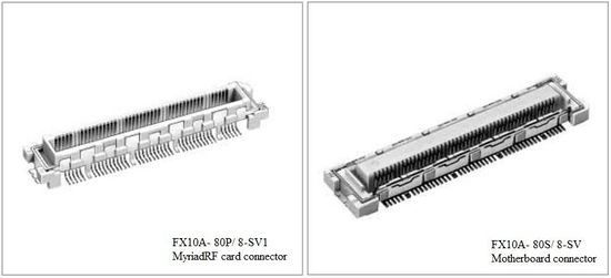
The connector is based on the Hirose 0.5 mm pitch, 80 positions, surface-mount connector. The female part number is FX10A-80S/8-SV, to be assembled on the motherboard. The male part number is FX10A-80P/8-SV1, and is to be used by the daughterboard. A typical example of use for an RF application is an Altera FPGA motherboard using a Myriad-RF daughterboard. This example will be used throughout this document for clarity.
Figure 1: Connector 3D View
Figure 1 shows the connectors in 3-D view.

Figure 2: Recommended PCB Footprint
Figure 2 shows the recommended land pattern (Metal Mask) connector dimensions.

A footprint for the open source EDA software, KiCad, is available via the database provided by the Component Libraries project.
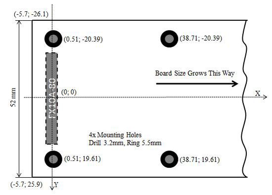
Figure 3: Myriad-RF 1 Card Mechanical Co-ordinates (Top View)
Figure 3 shows the dimensions of the Myriad-RF 1 daughterboard with the Hirose connector.

Electrical Specifications
Power
The carrier board must provide +5V (1.5A) DC to the RF card through the RFDIO connector. The maximum current via the Hirose connector is 0.3A per pin. To achieve the 1.5A specification, a number of defined supply and ground pins must be used. These are:
| +5V | Pin 1, 2, 3, 4, 8 & 10. |
| GND | Pin 5, 6, 11, 12, 17, 18, 27, 28, 37, 38, 47, 48, 57, 58, 62, 63, 73, 77, 81, 82, 83, 84, 85, 86, 87, 88, 89 & 90 |
CMOS Signals
The CMOS class pins are intended to connect directly to pins that support LVTTL compatible single-ended I/O standards such as 3.3-V LVTTL/LVCMOS or 2.5-V LVTTL/LVCMOS. All CMOS class pins must support bidirectional operation. Signals between the host FPGA device and HSMC connector are intended to be D/C coupled.
Bus Widths
Daughterboards must be designed to support the full specified bus widths. This will guarantee interoperability with the greatest number of RF cards.
Termination
Tracks must have 50 Ω single-ended impedances. An optimum design will be obtained if the host FPGA supports driver strength control where 50 Ω output impedances can be selected. This output impedance will match the characteristic impedance of the tracks themselves. For long track lengths or heavy loads, drive strength may be increased as necessary until optimal signal integrity is achieved for the specific carrier board or RF card combination. When impedance control is not possible, it is recommended to place series resistors on each line of the host board to allow for tuning through resistor value changes. Default resistors should be a nominal 0 Ω since signal direction cannot be assumed on a carrier board and higher value resistors found near a receiver can significantly degrade signal integrity.
Pinout
The RFDIO connector has a total of 90 pins, including 54 digital signals pins, 6 power pins, 2 analog pins and 28 ground pins.
| Pin Nr | Function | Description | Pin Nr | Function | Description |
|---|---|---|---|---|---|
| 1 | 5V | Power | 2 | 5V | Power |
| 3 | 5V | Power | 4 | 5V | Power |
| 5 | GND | Power | 6 | GND | Power |
| 7 | RSSI output | Analogue | 8 | 5V | Power |
| 9 | RSSI output | Analogue | 10 | 5V | Power |
| 81 | GND | Power | 82 | GND | Power |
| 11 | GND | Power | 12 | GND | Power |
| 13 | TXNRX2 | CMOS In | 14 | GPIO5 | CMOS IO |
| 15 | TXNRX1 | CMOS In | 16 | G_PWR_DWN | CMOS IN |
| 17 | GND | Power | 18 | GND | Power |
| 19 | ENABLE_IQSEL1 | CMOS In | 20 | GPIO6 | CMOS IO |
| 21 | SPI_EN_BRD | CMOS In | 22 | GPIO 7 | CMOS IO |
| 23 | DIQ1_D0 | CMOS IO | 24 | DIQ1_D1 | CMOS IO |
| 25 | DIQ1_D2 | CMOS IO | 26 | DIQ1_D3 | CMOS IO |
| 27 | GND | Power | 28 | GND | Power |
| 29 | DIQ1_D4 | CMOS IO | 30 | DIQ1_D5 | CMOS IO |
| 83 | GND | Power | 84 | GND | Power |
| 31 | DIQ1_D6 | CMOS IO | 32 | DIQ1_D7 | CMOS IO |
| 33 | DIQ1_D8 | CMOS IO | 34 | DIQ1_D9 | CMOS IO |
| 35 | DIQ1_D10 | CMOS IO | 36 | DIQ1_D11 | CMOS IO |
| 37 | GND | Power | 38 | GND | Power |
| 39 | ENABLE_IQSEL2 | CMOS In | 40 | BRDPRSNT | Board present, connects to GND on RF Card |
| 41 | GPIO4 | CMOS IO | 42 | VIO | Digital IOs supply |
| 43 | DIQ2_D0 | CMOS IO | 44 | DIQ2_D1 | CMOS IO |
| 45 | DIQ2-D2 | CMOS IO | 46 | DIQ2_D3 | CMOS IO |
| 47 | GND | Power | 48 | GND | Power |
| 49 | DIQ2_D4 | CMOS IO | 50 | DIQ2_D5 | CMOS IO |
| 85 | GND | Power | 86 | GND | Power |
| 51 | DIQ2_D6 | CMOS IO | 52 | DIQ2_D7 | CMOS IO |
| 53 | DIQ2_D8 | CMOS IO | 54 | DIQ2_D9 | CMOS IO |
| 55 | DIQ2_D10 | CMOS IO | 56 | DIQ2_D11 | CMOS IO |
| 57 | GND | Power | 58 | GND | Power |
| 59 | FCLK2 | CMOS CLK In | 60 | FCLK1 | CMOS CLK In |
| 61 | MCLK2 | CMOS CLK Out | 62 | GND | Power |
| 63 | GND | Power | 64 | MCLK1 | CMOS CLK Out |
| 65 | GPIO0 | CMOS In | 66 | RESET | CMOS In |
| 67 | GPIO1 | CMOS In | 68 | SPI_MOSI | CMOS In |
| 69 | GPIO2 | CMOS In | 70 | SPI_MISO | CMOS Out |
| 87 | GND | Power | 88 | GND | Power |
| 71 | GPIO3 | CMOS In | 72 | SPI_CLK | CMOS In |
| 73 | GND | Power | 74 | SPI_EN_LMS | CMOS In |
| 75 | CLK_IN | CMOS reference CLK input for RF Card | 76 | MIPI_SDA | CMOS IO |
| 77 | GND | Power | 78 | MIPI_SCL | CMOS in |
| 79 | TXEN | CMOS In | 80 | RXEN | CMOS In |
| 89 | GND | Power | 90 | GND | Power |
For complete signals description and timing diagrams refer to LMS6002D or LMS7002M datasheet.
See Also
- Reference Development Kit
- LMS6002D datasheet
- LMS7002M datasheet
- Reference Development Kit Project Page
| |||||||||||||||||||||