Myriad-RF 1 Connections
Basic Connections
The Myriad-RF 1 Board can be used as a standalone board or in conjunction with the DE0-Nano Interface Board or Zipper Interface Board for connection to a compatible FPGA development system.. The Myriad-RF board is connected to the interface board via a standard Hirose FX10A-80P connector, connecting its digital interface to the development kit. The following sections describe the Myriad-RF 1's on-board connections..
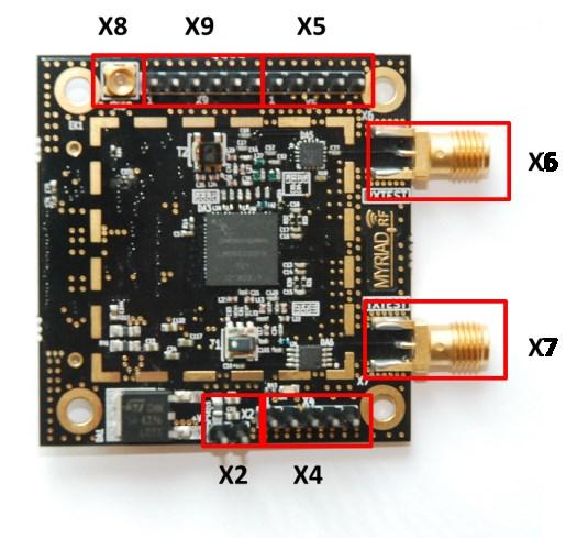
Myriad-RF 1 Board Connections
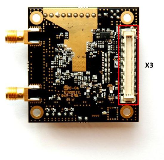
The analogue differential IQ interface is also available on Myriad-RF board and provided via X3 and X4 connectors. X6 and X7 are the RF connection for receive input and transmitter output on the RF board, see figure 3. The RF board is tuned to support band 1 (Tx 2140 MHz and Rx 1950 MHz) and broadband operation. The front end switches are configurable for selected receiver input and transmitter output via GPIOs. The GPIOs are controlled by the FPGA module.


The following table describes the pin assignment for each connector on the Myriad-RF 1 board.
| Connector | Name | Description |
|---|---|---|
| X2 | +5 V supply | External +5 V supply. |
| X3 | Digital IO | The FX10A-80P is a standard connector used to interface the
RF board directly to the interface board or any other baseband board. |
| X4 | TX Analogue I/Q | Connector used to supply Transmit analogue I/Q signals. |
| X5 | RX Analogue I/Q | Connector used to measure Receive analogue I/Q signals. |
| X6 | RXTEST | SMA connector providing connection to low band or high band RX input. Requires preselected RF switch configuration. |
| X7 | TXTEST | SMA connector that provides conection to low band or high band TX output. Requires preselected RF switch configuration. |
| X8 | Ext-CLK | Connector used to supply PLL clock externaly. Please refer to the GPIO Control Truth Table for more information. |
| X9 | Ext-SPI | Connector used to control LMS6002DFN SPI registers externally. SPI registers are controlled via X3 connector. Please refer to SPI Options for more information. |
X2 - +5 V Supply Connector
The pin header type connector used to supply +5 V to the Myriad-RF 1 board in standalone mode.
X3 - Digital IO Connector
The Myriad-RF board X3 connector (type FX10A-80P0) is pin compatible with the J1 connector on interface board. It provides the digital and SPI interface for the LMS6002DFN together with the supply voltage and GPIO control for the RF switches for the Myriad-RF 1 board. The pin descriptions on this connector are given in the table below:
| Pin Nr | Function | Type | Description |
|---|---|---|---|
| 1 | +5 V | In DC | +5 V power supply |
| 2 | +5 V | In DC | +5 V power supply |
| 3 | +5 V | In DC | +5 V power supply |
| 4 | +5 V | In DC | +5 V power supply |
| 5 | GND | Ground pin | |
| 6 | GND | Ground pin | |
| 7 | +3.3 V | In DC | +3.3 V power supply, optional |
| 8 | +3.3 V | In DC | +3.3 V power supply, optional |
| 9 | +3.3 V | In DC | +3.3 V power supply, optional |
| 10 | +3.3 V | In DC | +3.3 V power supply, optional |
| 11 | GND | Ground pin | |
| 12 | GND | Ground pin | |
| 13 | - | Not used | |
| 14 | - | Not used | |
| 15 | - | Not used | |
| 16 | - | Not used | |
| 17 | GND | Ground pin | |
| 18 | GND | Ground pin | |
| 19 | TXIQSEL | In CMOS | TX digital interface IQ flag |
| 20 | - | Not used | |
| 21 | - | Not used | |
| 22 | - | Not used | |
| 23 | TXD0 | In CMOS | DACs digital input, bit 0 (LSB) |
| 24 | TXD1 | In CMOS | DACs digital input, bit 1 |
| 25 | TXD2 | In CMOS | DACs digital input, bit 2 |
| 26 | TXD3 | In CMOS | DACs digital input, bit 3 |
| 27 | GND | Ground pin | |
| 28 | GND | Ground pin | |
| 29 | TXD4 | In CMOS | DACS digital input, bit 4 |
| 30 | TXD5 | In CMOS | DACS digital input, bit 5 |
| 31 | TXD6 | In CMOS | DACS digital input, bit 6 |
| 32 | TXD7 | In CMOS | DACS digital input, bit 7 |
| 33 | TXD8 | In CMOS | DACS digital input, bit 8 |
| 34 | TXD9 | In CMOS | DACS digital input, bit 9 |
| 35 | TXD10 | In CMOS | DACS digital input, bit 10 |
| 36 | TXD11 | In CMOS | DACS digital input, bit 11 |
| 37 | GND | Ground pin | |
| 38 | GND | Ground pin | |
| 39 | RXIQSEL | Out CMOS | RX digital interface IQ flag |
| 40 | - | Not used | |
| 41 | - | Not used | |
| 42 | - | Not used | |
| 43 | RXD0 | Out CMOS | ADCs digital output, bit 0 (LSB) |
| 44 | RXD1 | Out CMOS | ADCs digital output, bit 1 |
| 45 | RXD2 | Out CMOS | ADCs digital output, bit 2 |
| 46 | RXD3 | Out CMOS | ADCs digital output, bit 3 |
| 47 | GND | Ground pin | |
| 48 | GND | Ground pin | |
| 49 | RXD4 | Out CMOS | ADCs digital output, bit 4 |
| 50 | RXD5 | Out CMOS | ADCs digital output, bit 5 |
| 51 | RXD6 | Out CMOS | ADCs digital output, bit 6 |
| 52 | RXD7 | Out CMOS | ADCs digital output, bit 7 |
| 53 | RXD8 | Out CMOS | ADCs digital output, bit 8 |
| 54 | RXD9 | Out CMOS | ADCs digital output, bit 9 |
| 55 | RXD10 | Out CMOS | ADCs digital output, bit 10 |
| 56 | RXD11 | Out CMOS | ADCs digital output, bit 11 |
| 57 | GND | Ground Pin | |
| 58 | GND | Ground Pin | |
| 59 | RXCLK | In CMOS | RX digital interface clock |
| 60 | TXCLK | In CMOS | TX digital interface clock |
| 61 | - | Not used | |
| 62 | - | Not used | |
| 63 | GND | Ground pin | |
| 64 | GND | Ground pin | |
| 65 | GPIO0 | ||
| 66 | RESET | In CMOS | Hardware reset, active low |
| 67 | GPIO1 | ||
| 68 | SPI_MOSI | Out CMOS | Serial port data out |
| 69 | GPIO2 | ||
| 70 | SPIO_MISO | In/Out CMOS | Serial port data in/out |
| 71 | - | Not used | |
| 72 | SPI_CLK | In CMOS | Serial port clock, positive edge sensitive |
| 73 | GND | Ground pin | |
| 74 | SPI-NCSO | In CMOS | Serial port enable, active low |
| 75 | CLK_IN | In CMOS | PLL reference clock input |
| 76 | - | Not used | |
| 77 | GND | Ground pin | |
| 78 | - | Not used | |
| 79 | TXEN | In CMOS | Transmitter enable, active high |
| 80 | RXEN | In CMOS | Receiver enable, active high |
| 81 | GND | Ground pin | |
| 82 | GND | Ground pin | |
| 83 | GND | Ground pin | |
| 84 | GND | Ground pin | |
| 85 | GND | Ground pin | |
| 86 | GND | Ground pin | |
| 87 | GND | Ground pin | |
| 88 | GND | Ground pin |
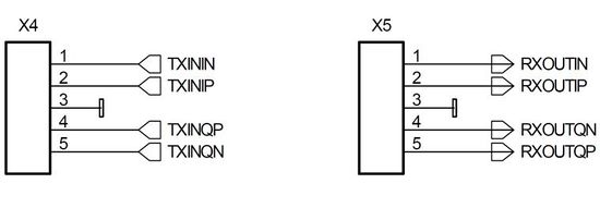
X4 and X5 - Analogue IQ Connectors
Pin header type connectors on the Myriad-RF 1 board, providing analogue IQ signal I/O.

| X4 | X5 | ||
|---|---|---|---|
| Pin Nr | Function | Pin Nr | Function |
| 1 | TXININ | 1 | RXOUTIN |
| 2 | TXINIP | 2 | RXOUTIP |
| 3 | 3 | ||
| 4 | TXINQP | 4 | RXOUTQN |
| 5 | TXINQN | 5 | RXOUTQP |
X6 and X7 - RF Input and Output
The X6 and X7 are SMA type connectors which provide Receive input and Transmit output to the LMS6002DFN, respectively. These are generally used to connect to antenna or test equipment.
X8 - External CLK Connector
The X8 is a micro miniature coaxial connector (MMCX8400). It is optional and used to supply external clock in standalone mode.
X9 - External SPI Connector
This is a pin header type connector used for SPI interface to LMS602DFN. This is optional, if the board is used in standalone mode.
SPI Options
The Myriad-RF 1 board offers two options for SPI communications: SPI communication is established via the FPGA and USB microcontroller located on the interface board; or SPI communication is established via the Myriad-RF 1's own USB microcontroller. In order to ensure stable SPI communication for your chosen option, the interface board may require a component change. Please note that NF denotes that component is not fitted:
| SPI Options | ||
|---|---|---|
| Components | SPI via FPGA | SPI via USB controller |
| R48 | NF | 0 Ohm |
| R58 | NF | 0 Ohm |
| R51 | NF | 0 Ohm |
| R46 | NF | 0 Ohm |
| R52 | NF | 0 Ohm |
GPIO Control Truth Table
The RF switches on the RF board are controlled via the GPIO0-2 logic signals, provided by the FPGA module on the interface board. This enables the user to choose RF input/output depending on the operation frequency. The truth table of the GPIO0-2 settings is shown below:
| LMS6002D RF Input/Output | GPIO0 | GPIO1 | GPIO2 | Description |
|---|---|---|---|---|
| TX Out 1 | X | X | 0 | High band output (1500 - 3800 MHz) |
| TX Out 2 | X | X | 1 | Broadband output |
| RX In 1 | 1 | 1 | X | Low band input (300 - 2200 MHz) |
| RX In 2 | 0 | 1 | X | High band input (1500 - 3800 MHz) |
| RX In 3 | 0 | 0 | X | Broadband input |
Standalone Mode
The Myriad-RF board can operate in standalone mode. Setup for standalone mode is as follows:
- Connect +5 V power supply to X2 connector on the Myriad-RF board.
- Connect SPI control to X9 connector.
- Connect wanted reference clock to X8 connector. Fit R49 resistor.
In this mode you are able to fully control the LMS6002DFN chip register and perform some basic RF measurements using IQ analogue inputs/outputs.