Getting Started with LimeSDR-USB and LimeSuiteGUI
Launching LimeSuiteGUI and Connecting to the Board
First of all, connect LimeSDR-USB board to PC USB3.0 socket. Please go Driver Installation Documentation to see how to install OS drivers so your PC can see LimeSDR-USB board. In the provided USB Flash there is a folder GUI in which you will find LimeSuiteGUI.exe file (or just download the software from here). Open it.
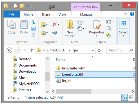
To launch LimeSuiteGUI application go to menu and select: Options -> Connection Settings as shown in Figure 2.
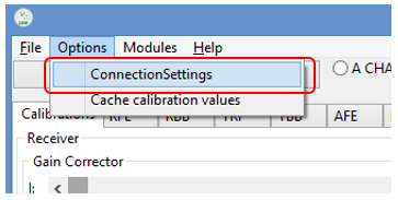
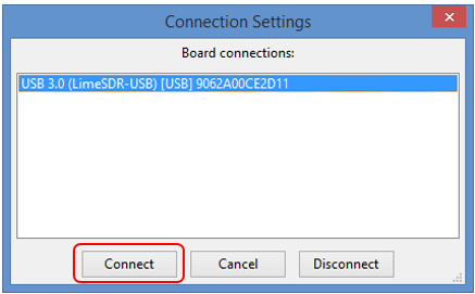
Select LimeSDR-USB board as shown in Figure 3 and press Connect.
Loading and Saving Register Settings
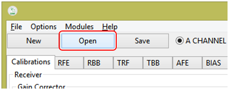
In order to load settings, click button Open as shown in Figure 4.
Select .ini setting file and click Open as shown in Figure 5.
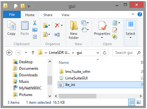
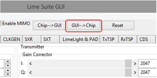
Then click GUI --> Chip button as shown in Figure 6.
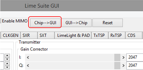
If you want load all LMS7002M settings from LimeSDR-USB to GUI, then click button Chip-->GUI as shown in Figure 7.
Quick Test
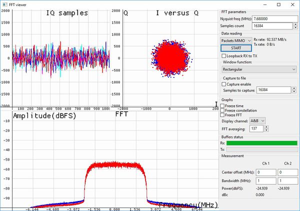
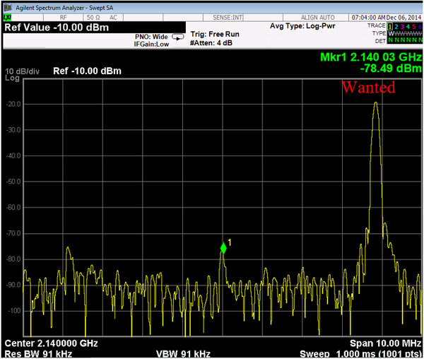
If there is a need to check if the board is fully working you can run very simple and quick board test. All instruction on how to do it you can find it in LimeSDR-USB Quick Test. One you see the graph as it show in Figure 8 of W-CDMA signal on FFT Viewer, you know that the board is working.
Changing TX / RX Frequency
After power up in order to configure LMS7002M Tx or Rx LO to 2140 MHz, do the following:
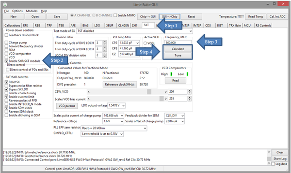
- Select the SXR tab for Receiver or SXT tab for Transmitter
- Enable SXR/SXT module
- Type the wanted frequency in Frequency, GHz box. In this case, 800 MHz
- Press Calculate followed by Tune
See Figure 9 to check related controls in the LimeSuiteGUI.
Changing Receiver Gain
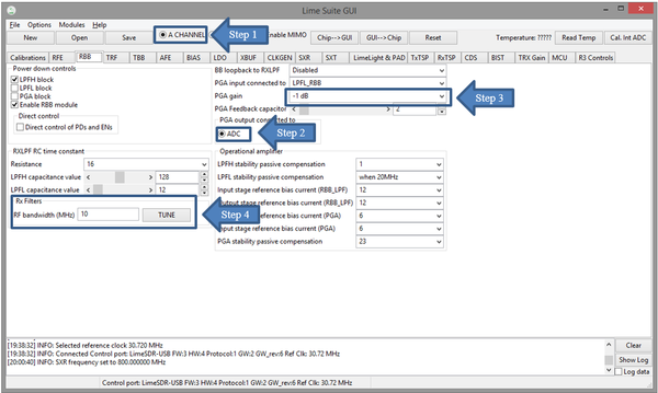
Select the RBB tab to configure the PGA gain and baseband filter bandwidths. Follow the configuration steps below:
- Select the A CHANNEL to control channel A
- Select PGA output to output pads. This selection enables receiver analog outputs
- Set PGA gain to -1 dB
- Configure filter bandwidth. Type desired bandwidth and click Tune
See Figure 10 below to check related controls in the LimeSuiteGUI.
Changing Transmitter Output Signal Gain
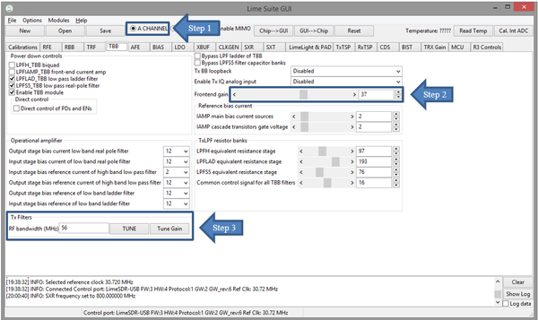
In the TBB tab the baseband gain and filter bandwidth are controlled. Follow the instructions below to set up TBB:
- Select the A CHANNEL to control channel A
- Set Frontend gain to your wanted
- Configure the base band filter settings. Type desired bandwidth and click Tune and Tune gain
See Figure 11 below to check related controls in the LimeSuiteGUI.
Load Waveform for Tx Path
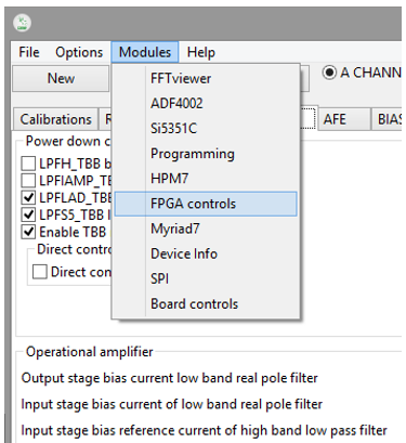
The programed FPGA is acting as waveform player for LMS7002M transceiver. In order to load the waveform, select Modules from top menu, then FPGA Controls from the drop down menu as shown in Figure 12.
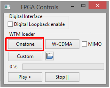
New window will appear in the bottom of the GUI, offering you to load supplied waveforms or custom waveforms. Please select to load CW waveform by clicking on Onetone button, as shown in Figure 13.
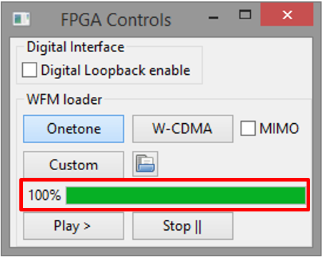
The file loading process to the FPGA is shown by indication bar, see Figure 14.
Digital Loopback Enable
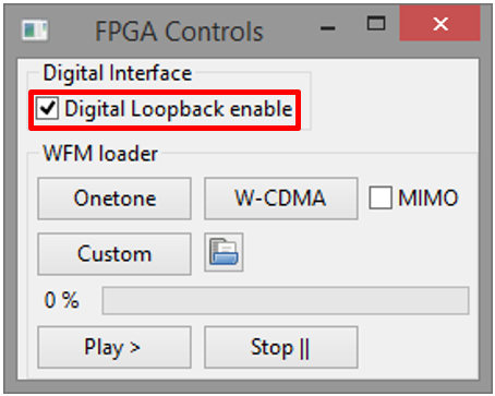
There is also implemented option to receive data from LMS7002M receiver and stream back on to LMS7002M transmitter. In order to enable this option, click on the ‘Digital Loopback enable’ check box in the ‘FPGA Control’ Module Figure 15.
Run FTT viewer
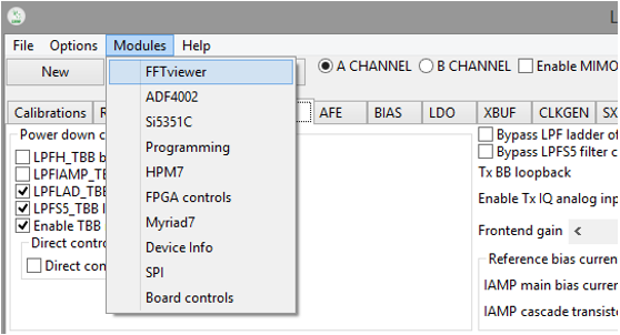
FFTviewer module is a part of LimeSuiteGUI software. To run FFTviewer, go to top menu, select Modules and choose FFTviewer as shown in Figure 16.
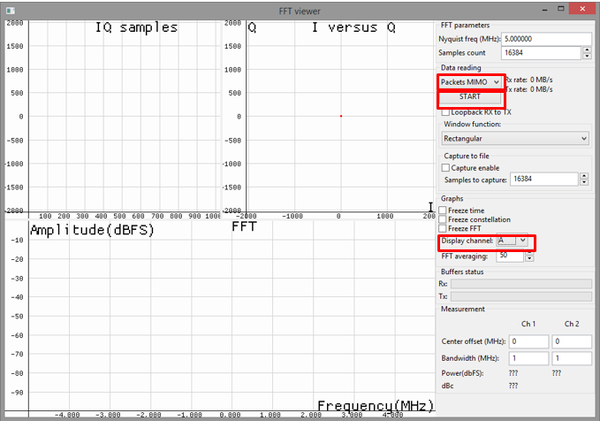
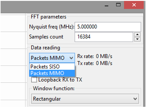
FFTviewer control window will appear. Before start capturing data, set the Data reading type to “Packets MIMO”, Display channel and press Start, as shown in Figure 17 and Figure 18.
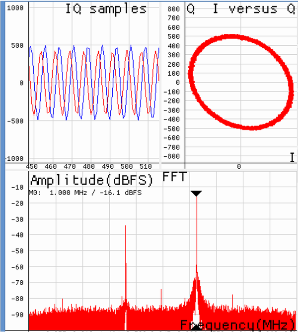
At this point, the FFTviewer start capturing data. Connect the generator to selected LimeSDR receiver path. In the Figure 19 showed the FFTviewer data capture with 1 MHz CW signal offset from LO.
Manual Calibration of RX Path
Rx DC offset and Rx Unwanted SSB calibration routines have to be executed to calibrate receiver path. The Rx DC offset calibration split in two parts; Analog DC Offset calibration and digital DC offset removal procedure.
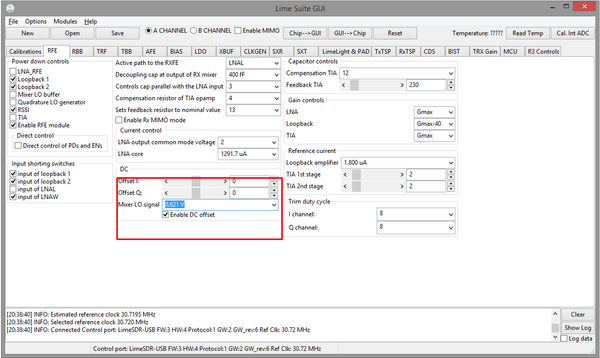
To execute Analog DC Offset calibration, select the RFE tab in the main GUI window. Make sure that you have selected channel A. In the DC box, change Mixer LO signal to 0.621 V and look for the best Offset I/Q values to reach minimum level of DC Offset. See Figure 20 below.
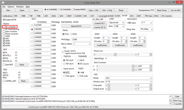
For residual DC offset calibration you need to enable the DC corrector in RxTSP tab. See Figure 21. It should be enabled (check box un-checked) by default.
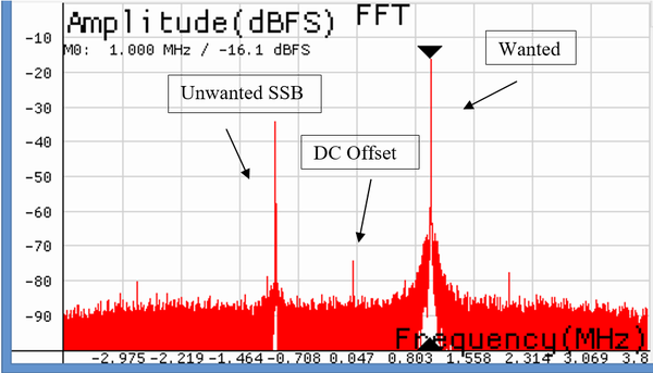
The unwanted SSB can be seen on FFTviewer window by applying signal to one of the transceiver inputs. See Figure 22.
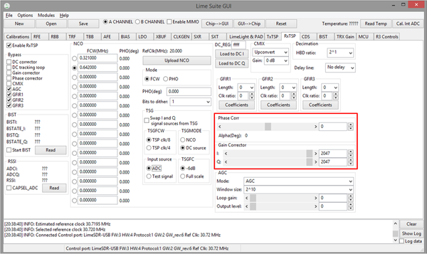
To calibrate RX IQ imbalance, go to RxTSP tab on LimeSuiteGUI GUI. On IQ Correction box adjust Gain ch. I or Gain ch. Q followed by Phase correction to reduce the Unwanted SSB. See Figure 23.
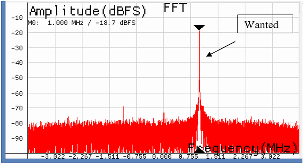
Calibrated receiver spectrum should look like in the Figure 24.
Manual Calibration of TX Path
The LO leakage and IQ imbalance have to be calibrated for the LMS7002M transceiver in order to get optimum performance for Tx EVM measurement. The IQ imbalance calibration is done by generating CW and adjusting IQ phase/gain error for IQ mismatch. Th LO leakage calibration is doem by adjust DC offset registers. The internal test NCO can be enabled for this purpose. To do this, select TxTSP tab in LimeSuiteGUI and select the Test Signal as input for Tx path and NCO as TSGMODE, as showed in figure below.
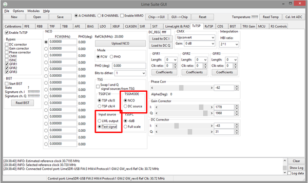
NOTE: Before configuring TxTSP tab, select the A/RXT channel in top right of the GUI.
On the transmitter output you should see the wanted CW with 3.8MHz offset from LO, unwanted SSB on the other side of spectrum and LO leakage. See Figure 26.
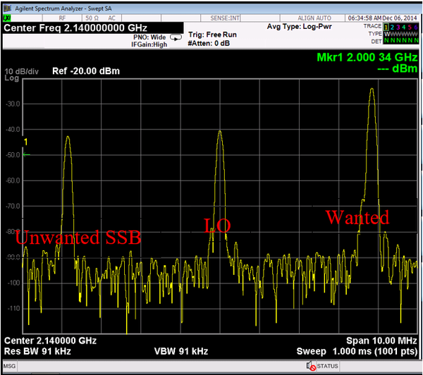
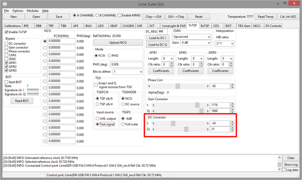
To do the LO leakage calibration, select TxTSP tab in the LimeSuiteGUI GUI and adjust the DC Corrector settings (see Figure 27) for channel I and Q separately to get minimum LO leakage.
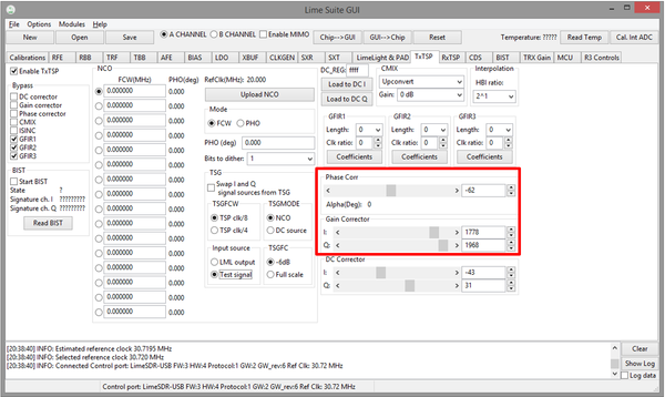
To calibrate Unwanted SSB, use the IQ Corrector controls in the TxTSP tab. Change I ch. gain or Q ch. gain followed by Phase correction to reduce the Unwanted SSB as shown in Figure 28.
Calibrated Transceiver TX output should look like in the Figure 29.
Once TX is calibrated the settings can be saved and can be recalled after chip power cycle. After calibration is complete and configure Tx path to accept data from Stream board; go to TxTSP and select LML output under Tx Input Source has to be selected to in TxTSP tab. See Figure 25.
NOTE: The Tx IQ and LO leakage calibration procedure can be done using auto calibration routines. The routines are accessed from Calibration tab in the GUI.
Clock configuration
Onboard clock sources can be configured by LimeSuiteGUI. More information about clock distribution is detailed in Clock distribution description.
VCTCXO tuning
VCTCXO can be tuned by onboard phase detector (IC23, ADF4002) or by DAC (IC22). The onboard phase detector is used to synchronize onboard VCTCXO with external equipment (via J19 U.FL connector) to calibrate frequency error. At the same time only phase detector or DAC can control VCTCXO. DAC and phase detector is controlled by FX3 (USB) and selection between them is done automatically. When board is powered, by default VCTCXO is controlled by DAC.
FPGA2 LED indicates DAC or phase detector controls VCTCXO and phase detector lock state. More information about LEDs can be found in Indication LEDs.
Tuning VCTCXO using frequency synthesizer (ADF4002)
VCTCXO can be tuned by onboard phase detector (IC23, ADF4002) or by DAC (IC22). If phase detector is configured from LimeSuiteGUI software, then DAC is disabled automatically and VCTCXO tuning voltage is supplied from phase detector. When phase detector controls VCTCXO, FPGA2 LED indicates its lock state: red – not locked, green – locked.
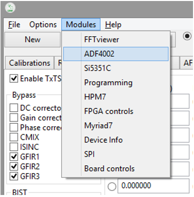
The phase detector is used to synchronize onboard VCTCXO with external equipment (via J19 U.FL connector) to calibrate frequency error and can be configured using LimeSuiteGUI software. Because VCTCXO also can be tuned by DAC, in this case DAC is disabled. Go to Modules form top menu and select ADF4002 form the drop down menu, as shown in Figure 30.
New control window should appear, as shown in the Figure 31.
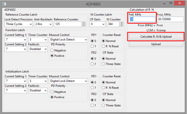
Field Fref value indicates the frequency to that VCTCXO will be synchronized and must be fed to REF_CLK (J14) connector. Usually this value is 10 MHz. When all parameters are entered in this window, press button Calculate R, N & Upload and frequency synthesizer will be configured.
Tuning VCTCXO using DAC
VCTCXO can be tuned by onboard frequency synthesizer (IC16, ADF4002) or by DAC (IC15). If DAC is configured from LimeSuiteGUI software, then frequency synthesizer is shut down and VCTCXO tuning voltage is supplied from DAC. When DAC controls VCTCXO, FPGA2 LED is off.
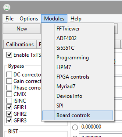
DAC can be configured using LimeSuiteGUI software. Go to Modules form top menu and select Board controls form the drop down menu, as shown in Figure 32.
New window will appear, as shown in the Figure 33.
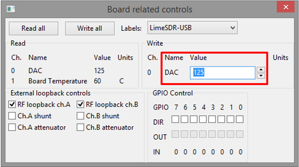
Current DAC value can be read by pressing button Read all. DAC value will be displayed in group box Read with channel 0. In this case DAC value is 125.
Enter new DAC value in group box Write channel 0. After this press Write all and DAC value will be updated.
VCTCXO calibration procedure
Board has VCTCXO DAC factory calibration value that is stored in non-volatile memory. This value is loaded to DAC output after each board power up or reset. This value can be changed manually or by automatic calibration procedure. To perform automatic calibration procedure, connect external reference clock to connector J19, start it from LimeSuiteGUI software and enter Fref frequency (default Fref value 10MHz).
Calibration procedure steps:
- Lock phase detector (ADF4002) to external Fref clock as described in section Error! Reference source not found. Error! Reference source not found.. If phase detector cannot lock to reference clock, calibration procedure cannot continue and will be aborted.
- Measure TCVCXO frequency and store for future comparison.
- Start changing TCXO DAC value and detect when VCTCXO frequency is as close as possible to the value measured in step 2.
- Store new VCTCXO value in non-volatile memory.
Programmable clock generator (Si5351C) configuration
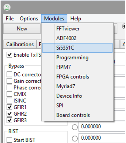
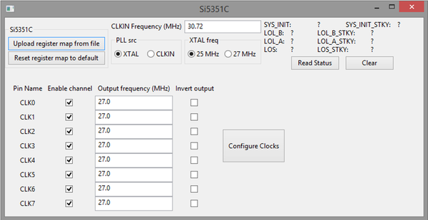
Programmable clock generator has eight channels and each can be configured individually using “LimeSuiteGUI”software. Go to Modules form top menu and select Si5351C form the drop down menu, as shown in Figure 34.
New window will appear, as shown in the Figure 35.
Reading board temperature
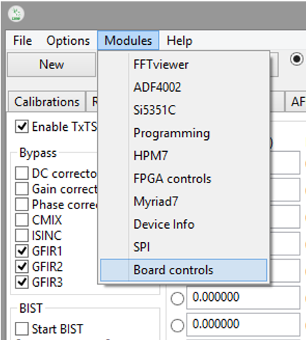
LimeSDR-USB has integrated temperature sensor. The sensor measured temperature may be displayed in software. Go to Modules form top menu and select Board controls form the drop down menu, as shown in Figure 36.
New window appears, as shown in the Figure 37.
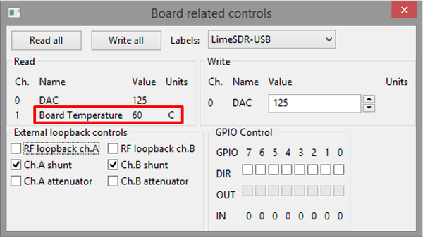
Current temperature sensor value can be read by pressing button Read all. Temperature value will be displayed in group box Read with channel 1. In this case temperature is 60 °C.
| |||||||||||||||||||||