LimeSDR-USB hardware description
LimeSDR-USB Board Key Features
The LimeSDR-USB development board provides a hardware platform for developing and prototyping high-performance and logic-intensive digital and RF designs using Altera’s Cyclone IV FPGA and Lime Microsystems transceiver.
The LimeSDR-USB has two different USB connector versions. LimeSDR-USB 1v4 is micro USB type B connector (socket) based, as shown in Figure 1. LimeSDR-USB 1v4s is a USB type A connector (plug) based, as shown in Figure 2.
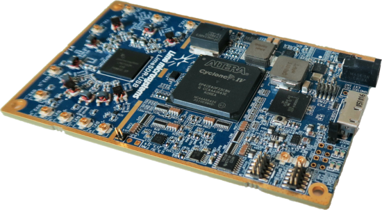
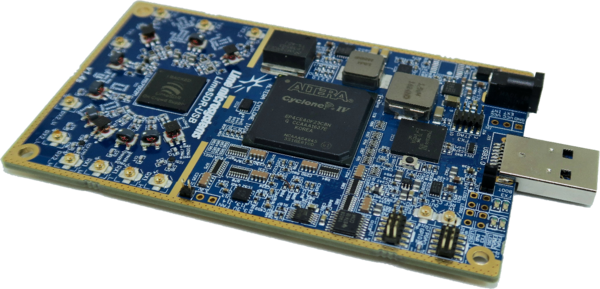
LimeSDR-USB board features:
- USB Interface
- Cypress FX3 Super Speed USB 3rd generation controller
- FPGA Features
- Cyclone IV EP4CE40F23C8N device in 484-pin FPGA
- 39’600 logic elements
- 1134 Kbits embedded memory
- 116 embedded 18x18 multipliers
- 4 PLLs
- FPGA Configuration
- JTAG mode configuration
- Active serial mode configuration
- Possibility to update FPGA gateware by using FX3 (USB)
- Memory Devices
- 2x 1Gbit (64M x 16) DDR2 SDRAM
- 4Mbit flash for FX3 firmware
- 16Mbit flash for FPGA gateware
- 2 x 128K (16K x 8) EEPROMs for LMS MCU firmware, LMS MCU data
- 1 x 64K (8K x 8) EEPROM for FX3 data
- Connections
- microUSB3.0 (type B) connector or USB3.0 (type A) plug
- Coaxial RF (U.FL) connectors
- FPGA GPIO headers (0.05” pitch)
- FPGA and FX3 JTAG connectors (0.05” pitch)
- 6..12V DC power jack and pinheader
- Fan connector (3.3V)
- Clock System
- 30.72MHz VCTCXO (precision: ±1 ppm initial, ±4 ppm stable).
- Possibility to lock VCTCXO to external clock or tune VCTCXO by onboard DAC
- Programmable clock generator for the FPGA reference clock input or LMS PLLs
- Board Size 60mm x 100mm (2.36” x 3.94”)
LimeSDR-USB board overview
LimeSDR-USB board version 1.4 picture with highlighted major connections presented in Figure 3. There are three connector types – data and debugging (USB3.0, FPGA GPIO and JTAG), power (DC jack and external supply pinheader) and high frequency (RF and reference clock).
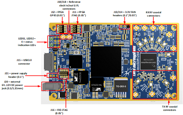
Board components description listed in the Table 1 and Table 2.
| Featured Devices | ||
|---|---|---|
| Board reference | Type | Description |
| IC1 | FPRF | Field programmable RF transceiver, LMS7002M |
| IC8 | FPGA | Altera Cyclone IV, EP4CE40F23C8N 484-BGA |
| IC13 | USB 3.0 microcontroller | Cypress FX3 Super Speed USB 3rd generation controller, CYUSB3014 |
| Miscellaneous devices onboard | ||
| IC9 | IC | Quad SPDT switch, TS3A5018PW |
| IC6 | IC | Temperature sensor, LM75 |
| IC19 | IC | SPI to I²C bridge, SC18IS602BIPW (not mounted) |
| IC17 | IC | I²C port expander with 4 push-pull outputs and 4 inputs, MAX7322ATE+ |
| Configuration, Status and Setup Components | ||
| IC9 | IC | Quad SPDT switch, TS3A5018PW |
| R51, R52, R53, R54, R56, R57, R59, R60 | 0 Ohm resistor | FPGA (IC31) MSEL[3:0]. Default mode: Active Serial Standard configuration |
| R115, R116, R117 | 10 kOhm resistor | USB3.0 microcontroller (IC13) boot configuration (PMODE0[2:0]) resistors. Default mode: SPI boot, On Failure - USB Boot |
| R125, R127, R128 | 10 kOhm resistor | USB3.0 microcontroller (IC13) crystal/clock frequency selection (FSLC[2:0]) resistors. Default mode: 19.2MHz crystal |
| J16 | JTAG chain pin header | USB3.0 (IC6) microcontroller’s debugging pin header, 0.05” pitch |
| J17, R122 | Pin header | USB3.0 microcontroller boot source (Flash memory or USB), 0.05” pitch jumper or 0402 0R resistor. In normal operation jumper or resistor must be placed. |
| SW1 | Push-button | USB3.0 microcontroller reset button |
| J11 | JTAG chain pin header | FPGA programming pin header for Altera USB-Blaster download cable, 0.05” pitch |
| LEDS1 | Red-green status LEDs | User defined FPGA indication LED1 (near board edge if SMD; on the bottom if through-hole), User defined FPGA indication LED2 (farther board edge if SMD; on the top if through-hole) |
| LEDS2 | Red-green status LEDs | FX3 (USB) status indication LED (near board edge if SMD; on the bottom if through-hole), board power indication LED (farther board edge if SMD; on the top if through-hole) |
| General User Input/Output | ||
| J12 | Pin header | 8 FPGA GPIOs, 0.05” pitch |
| J13, J14 | Pin header | 3.3V fan connection pin headers, 0.1” and 0.05” pitch respectively |
| Memory Devices | ||
|---|---|---|
| Board reference | Type | Description |
| IC11, IC12 | DDR2 memory | 1Gbit (64M x 16) DDR2 SDRAM with a 16-bit data bus |
| IC2, IC3 | EEPROM | 128K (16K x 8) EEPROM, LMS7002 MCU firmware, LMS7002M data |
| IC18 | EEPROM | 64K (8K x 8) EEPROM, connected to main I2C bus |
| IC10 | Flash memory | 16Mbit Flash for FPGA configuration |
| IC15 | Flash memory | 4Mbit Flash for FX3 firmware |
| Communication Ports | ||
| J15 | USB3.0 connector | microUSB3.0 (type B) connector or USB3.0 (type A) plug |
| Clock Circuitry | ||
| XO1, XO2 | VCTCXO | 30.72MHz voltage-controlled crystal oscillator |
| IC24 | IC | Programmable clock generator for the FPGA reference clock input and RF boards |
| IC23 | IC | ADF4002 phase detector |
| IC22 | IC | DAC for TCXO (XT4) frequency tuning |
| J19 | U.FL connector | Reference clock input |
| J18 | U.FL connector | Reference clock output |
| Power Supply | ||
| J20 | DC input jack | External 6V..12V DC power supply |
| J21 | Pin header | External 6V..12V DC power supply and main internal power rail |
LimeSDR-USB board version 1.4 picture with highlighted top components are presented in Figure 4.
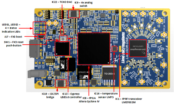
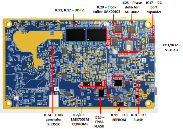
LimeSDR-USB board version 1.4 picture with highlighted bottom components is presented in Figure 5.
LimeSDR-USB board architecture
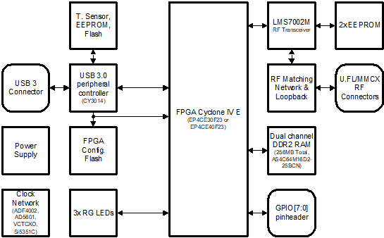
The heart of the LimeSDR-USB board is Altera Cyclone IV FPGA. Its main function is to transfer digital data between the PC through a USB3.0 connector. The block diagram for LimeSDR-USB board is presented in the Figure 6.
LMS7002M based connectivity
The interface and control signals are described below:
- Digital Interface Signals: LMS7002 is using data bus LMS_DIQ1_D[11:0] and LMS_DIQ2_D[11:0], LMS_ENABLE_IQSEL1 and LMS_ENABLE_IQSEL2, LMS_FCLK1 and LMS_FCLK2, LMS_MCLK1 and LMS_MCLK2 signals to transfer data to/from FPGA. Indexes 1 and 2 indicate transceiver digital data PORT-1 or PORT-2. Any of these ports can be used to transmit or receive data. By default, PORT-1 is selected as transmit port and PORT-2 is selected as receiver port. The FCLK# is input clock and MCLK# is output clock for LMS7002M transceiver. TXNRX signals sets ports directions. For LMS7002M interface timing details refer to LMS7002M transceiver datasheet.
- LMS Control Signals: these signals are used for optional functionality:
- LMS_RXEN, LMS_TXEN – receiver and transmitter enable/disable signals connected to FPGA Bank 8 (VDIO_LMS_FPGA; 2.5V).
- LMS_RESET – LMS7002M reset connected to FPGA Bank 7 (VDIO_LMS_FPGA; 2.5V).
- SPI Interface: LMS7002M transceiver is configured via 4-wire SPI interface; FPGA_SPI0_SCLK, FPGA_SPI0_MOSI, FPGA_SPI0_MISO, FPGA_SPI0_LMS_SS. The SPI interface controlled from FPGA Bank 8 (VDIO_LMS_FPGA; 2.5V).
- Main I2C Interface: used to control external clock synthesizer, port expander, temperature sensor, EEPROM, I2C-SPI bridge on LimeSDR-USB board. The signals FX3_I2C_SCL, FX3_I2C_SDA connected to FX3. Also these I2C lines are connected via 0R resistors to FPGA Bank 8 (VCC3P3; 3.3V) lines FPGA_I2C_SCL, FPGA_I2C_SDA.
- LMS I2C Interface: can be used for LMS EEPROM content modifying or for debug purposes. The signals LMS_I2C_SCL, LMS_I2C_DATA connected to FPGA Bank 8 (VDIO_LMS_FPGA; 2.5V).
SDRAM
LimeSDR-USB board has two 128MB (16bit bus) DDR2 SDRAM ICs (AS4C64M16D2-25BCN) connected to double data rate pins on Cyclone IV 1.8V Bank 2, Bank 3 and Bank 4. RAM chips are connected to separate memory controllers so RAM chips works in dual channel mode. The memory can be used for data manipulation at high date rates between transceiver and FPGA.
USB 3.0 controller
Software controls LimeSDR-USB board via the USB3 microcontroller (CYUSB3014 (FX3)). The data transfer to/from the board, SPI communication, FPGA configuration is done via the USB3 controller. The controller signals description showed below:
- FX3_DQ[31:0] – FX3 32-bit GPIF data interface is connected to Cyclone IV 1.8V Bank 5.
- FX3_CTL[8:0], [12:11] – FX3 GPIF interface control signals.
- FX3_PCLK – GPIF interface clock. Clock from FX3 is fed to FPGA.
- FX3_SPI interface is used to program FX3 firmware flash or FPGA configuration flash memory.
- FX3 I2C bus is connected to the main I2C bus.
- PMODE[2:0] – boot options, by default boot from SPI and USB boot is enabled. If J17 jumper is present or R122 is soldered FX3 will boot from IC8 flash memory if correct firmware exists.
- SW1 – resets FX3
- J16 – FX3 JTAG programming/debugging pin header.
Indication LEDs
LimeSDR-USB board comes with four dual colour (red and green (RG)) indication LEDs. These LEDs can be SMD or 3mm TH with dedicated right angle plastic holders. By default, dual colour SMD LEDs are populated and through hole LEDs are unpopulated. If required, the user can fit dual colour TH LEDs.
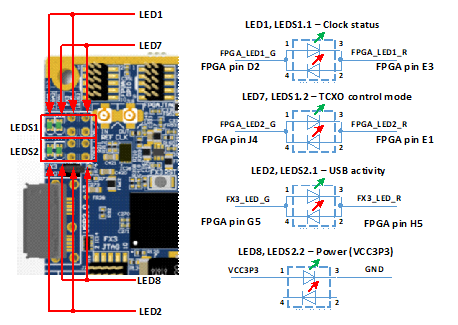
Each LED has it is own function. Most of LEDs are connected to FPGA and their function can be changed. Default LEDs functions and other information are listed in the table below.
| Board reference | Schematic name | Board label | Type | Description |
|---|---|---|---|---|
| LED8, LEDS2.2 | GND, VCC3P3 | PWR | Power status | LED is hardwired to VCC3P3 power rail. Steady green light indicates presence of 3.3v. |
| LED2, LEDS2.1 | FX3_LED_R, FX3_LED_G | FX3 | USB activity | USB3.0 (FX3) controller, slave FIFO (GPIF) interface module and NIOS CPU activity indication:
Green – idle, Red – busy. |
| LED1, LEDS1.1 | FPGA_LED1_G, FPGA_LED1_R | FPGA1 | Clock status | Blinking indicates presence of TCXO clock.
Colour indicates status of FPGA PLLs that are used for LMS digital interface clocking: Green – both PLLs are locked; Red/Green – at least one PLL is not locked. |
| LED7, LEDS1.2 | FPGA_LED2_G, FPGA_LED2_R | FPGA2 | TCXO control mode | No light – TCXO is controlled from DAC
Red – TCXO is controlled from phase detector and is not locked to external reference clock Green – TCXO is controlled from phase detector and is locked to external reference clock |
Low speed interfaces
LimeSDR-USB board low speed interfaces are divided into FX3 and FPGA groups that are presented in Figure 3, Figure 8 and Figure 9. The latter block diagrams depict the main ICs, corresponding IC pin numbers, data buses and serial protocol addresses.
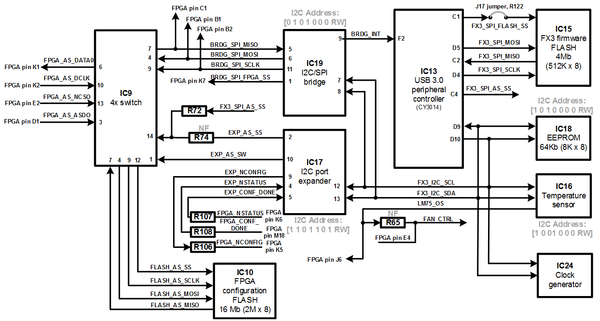
LimeSDR-USB board peripherals are controlled via USB interface. All commands that comes from USB are firstly processed by FX3 controller. If I2C peripheral (temperature sensor, port expander, clock generator) on FX3_I2C bus must be controlled this can be done directly. FX3_I2C is also connected to FPGA.
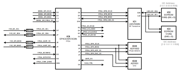
There are several SPI interfaces with their slave devices:
- FX3_SPI: FX3 hardware SPI cannot be used if 32-bit GPIF interface is configured. If any slave device on this bus must be accessed then FX3 switches to 16-bit GPIF. This bus has these slave devices:
- FX3 firmware Flash
- FPGA configuration flash: using switch (IC9) flash memory is switched from FPGA to FX3_SPI BUS. Then flash content is updated and flash memory is switch back to FPGA. This is done when needs to update FPGA gateware in flash memory.
- FPGA_SPI0, FPGA_SPI1: these SPI interfaces are connected to FPGA and slave devices can be accessed by transferring data to internal FPGA NIOS CPU. This bus has these slave devices:
- RFIC (FPGA_SPI0)
- Phase detector (FPGA_SPI1)
- DAC (FPGA_SPI1)
- Internal FPGA SPI module: FPGA has its own SPI module and can be controlled as regular SPI device. By using FPGA SPI it is possible to control FPGA modes etc.
- BRDG_SPI: this is alternative SPI interface for FX3 and currently is not used.
In the table below are listed USB3.0 controller (FX3) pins, schematic signal name, FPGA interconnections and I/O standard.
| FX3 | FX3 reference | Schematic signal name | FPGA pin | FPGA pin I/O standard | Comment |
|---|---|---|---|---|---|
| F10 | GPIO0 | FX3_DQ0 | M19 | 1.8V | |
| F9 | GPIO1 | FX3_DQ1 | AA21 | 1.8V | |
| F7 | GPIO2 | FX3_DQ2 | Y22 | 1.8V | |
| G10 | GPIO3 | FX3_DQ3 | Y21 | 1.8V | |
| G9 | GPIO4 | FX3_DQ4 | W22 | 1.8V | |
| F8 | GPIO5 | FX3_DQ5 | W21 | 1.8V | |
| H10 | GPIO6 | FX3_DQ6 | W20 | 1.8V | |
| H9 | GPIO7 | FX3_DQ7 | V22 | 1.8V | |
| J10 | GPIO8 | FX3_DQ8 | V21 | 1.8V | |
| J9 | GPIO9 | FX3_DQ9 | U22 | 1.8V | |
| K11 | GPIO10 | FX3_DQ10 | U21 | 1.8V | |
| L10 | GPIO11 | FX3_DQ11 | U20 | 1.8V | |
| K10 | GPIO12 | FX3_DQ12 | U19 | 1.8V | |
| K9 | GPIO13 | FX3_DQ13 | M22 | 1.8V | |
| J8 | GPIO14 | FX3_DQ14 | M21 | 1.8V | |
| G8 | GPIO15 | FX3_DQ15 | R22 | 1.8V | |
| J6 | GPIO16 | FX3_PCLK | T21 | 1.8V | |
| K8 | GPIO17 | FX3_CTL0 | L6 | 1.8V | |
| K7 | GPIO18 | FX3_CTL1 | L7 | 1.8V | |
| J7 | GPIO19 | FX3_CTL2 | M1 | 1.8V | |
| H7 | GPIO20 | FX3_CTL3 | M2 | 1.8V | |
| G7 | GPIO21 | FX3_CTL4 | M3 | 1.8V | |
| G6 | GPIO22 | FX3_CTL5 | M4 | 1.8V | |
| K6 | GPIO23 | FX3_CTL6 | M6 | 1.8V | |
| H8 | GPIO24 | FX3_CTL7 | M7 | 1.8V | |
| G5 | GPIO25 | FX3_CTL8 | M8 | 1.8V | |
| H6 | GPIO26 | FX3_DCTL9 | P9 | 1.8V | |
| K5 | GPIO27 | FX3_DCTL10 | N7 | 1.8V | |
| J5 | GPIO28 | FX3_CTL11 | N5 | 1.8V | |
| H5 | GPIO29 | FX3_CTL12 | N6 | 1.8V | |
| G4 | GPIO30 | FX3_PMODE0 | - | 1.8V | |
| H4 | GPIO31 | FX3_PMODE1 | - | 1.8V | |
| L4 | GPIO32 | FX3_PMODE2 | - | 1.8V | |
| K2 | GPIO33 | FX3_DQ16 | R21 | 1.8V | |
| J4 | GPIO34 | FX3_DQ17 | R20 | 1.8V | |
| K1 | GPIO35 | FX3_DQ18 | R19 | 1.8V | |
| J2 | GPIO36 | FX3_DQ19 | R18 | 1.8V | |
| J3 | GPIO37 | FX3_DQ20 | P22 | 1.8V | |
| J1 | GPIO38 | FX3_DQ21 | P21 | 1.8V | |
| H2 | GPIO39 | FX3_DQ22 | M20 | 1.8V | |
| H3 | GPIO40 | FX3_DQ23 | P16 | 1.8V | |
| F4 | GPIO41 | FX3_DQ24 | P15 | 1.8V | |
| G2 | GPIO42 | FX3_DQ25 | N22 | 1.8V | |
| G3 | GPIO43 | FX3_DQ26 | N21 | 1.8V | |
| F3 | GPIO44 | FX3_DQ27 | N20 | 1.8V | |
| F2 | GPIO45 | BRDG_INT_LS | - | 1.8V | Connected to I2C-SPI bridge |
| F5 | GPIO46 | FX3_DQ28 | N19 | 1.8V | |
| E1 | GPIO47 | FX3_DQ29 | N18 | 1.8V | |
| E5 | GPIO48 | FX3_DQ30 | N17 | 1.8V | |
| E4 | GPIO49 | FX3_DQ31 | N16 | 1.8V | |
| D1 | GPIO50 | - | - | 1.8V | |
| D2 | GPIO51 | - | - | 1.8V | |
| D3 | GPIO52 | - | - | 1.8V | |
| D4 | GPIO53 | FX3_SPI_SCLK | - | 3.3V | |
| C1 | GPIO54 | FX3_SPI_FLASH_SS | - | 3.3V | |
| C2 | GPIO55 | FX3_SPI_MISO | - | 3.3V | |
| D5 | GPIO56 | FX3_SPI_MOSI | - | 3.3V | |
| C4 | GPIO57 | - | - | 3.3V | |
| D9 | I2C_GPIO58 | FX3_I2C_SCL/FPGA_I2C_SCL | H7 | 3.3V | Connected to I2C-SPI bridge |
| D10 | I2C_GPIO59 | FX3_I2C_SDA/FPGA_I2C_SDA | J7 | 3.3V | Connected to I2C-SPI bridge |
In the table below are listed RF transceiver (LMS7002M) pins, schematic signal name, FPGA interconnections and I/O standard.
| LMS7002M pin | LMS7002M reference | Schematic signal name | FPGA pin | FPGA pin I/O standard | Comment |
|---|---|---|---|---|---|
| AM24 | xoscin_rx | RxPLL_CLK | - | 3.3V | Connected to 30.72 MHz clock |
| P34 | MCLK2 | LMS_MCLK2 | B11 | 2.5V | |
| R29 | FCLK2 | LMS_FCLK2 | E5 | 2.5V | |
| U31 | TXNRX2 | LMS_TXNRX2 | B8 | 2.5V | |
| V34 | RXEN | LMS_RXEN | C3 | 2.5V | |
| R33 | ENABLE_IQSEL2 | LMS_ENABLE_IQSEL2 | C7 | 2.5V | |
| H30 | DIQ2_D0 | LMS_DIQ2_D0 | B7 | 2.5V | |
| J31 | DIQ2_D1 | LMS_DIQ2_D1 | B6 | 2.5V | |
| K30 | DIQ2_D2 | LMS_DIQ2_D2 | B4 | 2.5V | |
| K32 | DIQ2_D3 | LMS_DIQ2_D3 | B3 | 2.5V | |
| L31 | DIQ2_D4 | LMS_DIQ2_D4 | A10 | 2.5V | |
| K34 | DIQ2_D5 | LMS_DIQ2_D5 | A9 | 2.5V | |
| M30 | DIQ2_D6 | LMS_DIQ2_D6 | A8 | 2.5V | |
| M32 | DIQ2_D7 | LMS_DIQ2_D7 | A7 | 2.5V | |
| N31 | DIQ2_D8 | LMS_DIQ2_D8 | A6 | 2.5V | |
| N33 | DIQ2_D9 | LMS_DIQ2_D9 | A5 | 2.5V | |
| P30 | DIQ2_D10 | LMS_DIQ2_D10 | A4 | 2.5V | |
| P32 | DIQ2_D11 | LMS_DIQ2_D11 | A11 | 2.5V | |
| E5 | xoscin_tx | TxPLL_CLK | - | 3.3V | Connected to 30.72 MHz clock |
| AB34 | MCLK1 | LMS_MCLK1 | G21 | 2.5V | |
| AA33 | FCLK1 | LMS_FCLK1 | B20 | 2.5V | |
| V32 | TXNRX1 | LMS_TXNRX1 | B9 | 2.5V | |
| U29 | TXEN | LMS_TXEN | B10 | 2.5V | |
| Y32 | ENABLE_IQSEL1 | LMS_ENABLE_IQSEL1 | C4 | 2.5V | |
| AG31 | DIQ1_D0 | LMS_DIQ1_D0 | B17 | 2.5V | |
| AF30 | DIQ1_D1 | LMS_DIQ1_D1 | B16 | 2.5V | |
| AF34 | DIQ1_D2 | LMS_DIQ1_D2 | B15 | 2.5V | |
| AE31 | DIQ1_D3 | LMS_DIQ1_D3 | B14 | 2.5V | |
| AD30 | DIQ1_D4 | LMS_DIQ1_D4 | B13 | 2.5V | |
| AC29 | DIQ1_D5 | LMS_DIQ1_D5 | C13 | 2.5V | |
| AE33 | DIQ1_D6 | LMS_DIQ1_D6 | A18 | 2.5V | |
| AD32 | DIQ1_D7 | LMS_DIQ1_D7 | A17 | 2.5V | |
| AC31 | DIQ1_D8 | LMS_DIQ1_D8 | A16 | 2.5V | |
| AC33 | DIQ1_D9 | LMS_DIQ1_D9 | A15 | 2.5V | |
| AB30 | DIQ1_D10 | LMS_DIQ1_D10 | A14 | 2.5V | |
| AB32 | DIQ1_D11 | LMS_DIQ1_D11 | A13 | 2.5V | |
| U33 | CORE_LDO_EN | LMS_CORE_LDO_EN | B18 | 2.5V | |
| E27 | RESET | LMS_RESET | C6 | 2.5V | |
| D28 | SEN | FPGA_SPI0_LMS_SS | D10 | 2.5V | SPI interface |
| C29 | SCLK | FPGA_SPI0_SCLK | E6 | 2.5V | SPI interface |
| F30 | SDIO | FPGA_SPI0_MOSI | D7 | 2.5V | SPI interface |
| F28 | SDO | FPGA_SPI0_MISO | C8 | 2.5V | SPI interface |
| D26 | SDA | LMS_I2C_SDA | C21 | 2.5V | Connected to EEPROM too |
| C27 | SCL | LMS_I2C_SCL | C17 | 2.5V | Connected to EEPROM too |
SPI interfaces, connected to the FPGA are listed in the tables bellow.
| Schematic net name | FPGA pin | I/O standard | Comment |
|---|---|---|---|
| FPGA_SPI0_SCLK | E6 | 2.5V | Serial Clock (FPGA output) |
| FPGA_SPI0_MOSI | D7 | 2.5V | Data (FPGA output) |
| FPGA_SPI0_MISO | C8 | 2.5V | Data (FPGA input) |
| FPGA_SPI0_LMS_SS | D10 | 2.5V | IC1 (LMS7002M) SPI slave select |
FX3 MCU features I2C interface. Slave devices and related information, connected to this interface, are listed in the table bellow.
| I2C slave device reference | I2C slave device | I2C slave address | I/O standard | Comment |
|---|---|---|---|---|
| IC9 | Temperature sensor | 1001000RW | 3.3V | LM75 |
| IC12 | I2C SPI Bridge | 0101000RW | 3.3V | SC18IS602B |
| IC10 | I2C Port Expander | 1101101RW | 3.3V | MAX7322 |
| IC11 | EEPROM | 1010000RW | 3.3V | 24FC64F |
| IC17 | Clock generator | 1100000RW | 3.3V | Si5351C |
Eight GPIOs from FPGA are connected to 10 pin 0.05” header. Additional 2 pins are dedicated for power. FPGA_GPIO related information is presented in the table below.
| Connector pin | Schematic net name | FPGA pin | I/O standard | Comment |
|---|---|---|---|---|
| 1 | FPGA_GPIO0 | H8 | 3.3V | |
| 2 | FPGA_GPIO1 | H6 | 3.3V | |
| 3 | FPGA_GPIO2 | H2 | 3.3V | |
| 4 | FPGA_GPIO3 | H1 | 3.3V | |
| 5 | FPGA_GPIO4 | G4 | 3.3V | |
| 6 | FPGA_GPIO5 | G3 | 3.3V | |
| 7 | FPGA_GPIO6 | F2 | 3.3V | |
| 8 | FPGA_GPIO7 | F1 | 3.3V | |
| 9 | GND | - | - | |
| 10 | PWR | - | - | Selectable power net. Default 3.3V |
Board temperature control
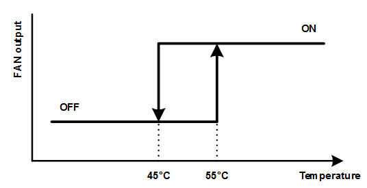
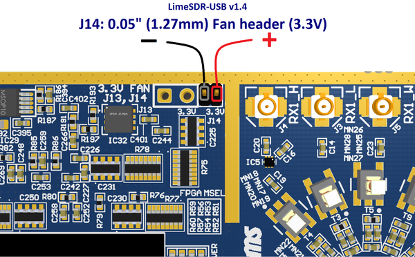
LimeSDR-USB has integrated temperature sensor which controls FAN to keep board in operating temperature range. FAN must be connected to J13 (0.1” pitch) connector or to J14 (0.05” pitch) connector. FAN control voltage is 3.3V.
Fan will be turned on if board will heat up to 55°C and FAN will be turned off if board will cool down to 45°C.
Measured temperature value can read by using LimeSuiteGUI.
Connect the fan as shown in the picture bellow.
Clock distribution
LimeSDR-USB board clock distribution block diagram is presented in Figure 12.
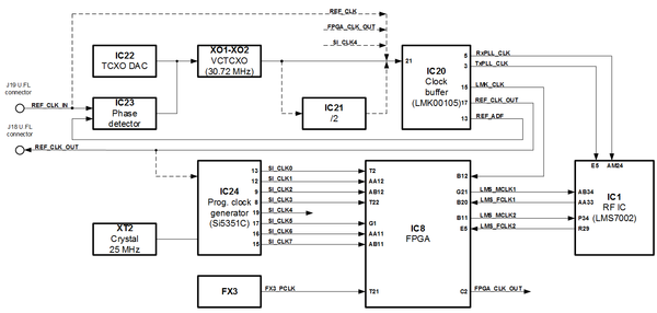
LimeSDR-USB board has onboard 30.72 MHz VCTCXO (precision: ±1 ppm initial, ±4 ppm stable) that is reference clock for LMS_PLLs. See block diagram of the clock distribution system in Figure 12.
VCTCXO can be tuned by onboard phase detector (IC23, ADF4002) or by DAC (IC22). The onboard frequency synthesizer is used to synchronize onboard VCTCXO with external equipment (via J19 U.FL connector) to calibrate frequency error. At the same time only ADF or DAC can control VCTCXO. Selection between ADF and DAC is done automatically. When board is powered, by default VCTCXO is controlled by DAC.
J19 connector can also be used to supply external reference clock (fitting R147, removing R137, C354).
The programmable clock generator (Si5351C) can generate any reference clock frequency, starting from 8 kHz – 160 MHz, for FPGA and LMS PLLs.
| Source | Schematic net name | FPGA pin | I/O standard | Comment |
|---|---|---|---|---|
| Programmable clock generator (IC24) | SI_CLK0 | T2 | 1.8V | |
| SI_CLK1 | AA12 | 1.8V | ||
| SI_CLK2 | AB12 | 1.8V | ||
| SI_CLK3 | T22 | 1.8V | ||
| SI_CLK5 | G1 | 3.3V | ||
| SI_CLK6 | AA11 | 1.8V | ||
| SI_CLK7 | AB11 | 1.8V | ||
| Clock buffer (IC13) | LMK_CLK | B12 | 3.3V | 30.72MHz |
| RF transceiver (IC1) | LMS_MCLK1 | G21 | 3.3V | |
| LMS_FCLK1 | B20 | 3.3V | ||
| LMS_MCLK2 | B11 | 3.3V | ||
| LMS_FCLK2 | E5 | 3.3V | ||
| USB3.0 controller | FX3_PCLK | T21 | 1.8V | |
| FPGA_CLK_OUT | C2 | 3.3V |
Power distribution
LimeSDR-USB board can be powered from USB port. In applications where USB power is insufficient board can be powered from external 6..12V power supply. External power supply can be fed to J20 barrel power connector by using power plug (1.35mm ID, 3.5mm OD) or pin header J21 (GND and VCC_EXT). External power supply connections have automatic source selection between USB and external source with polarity protection.
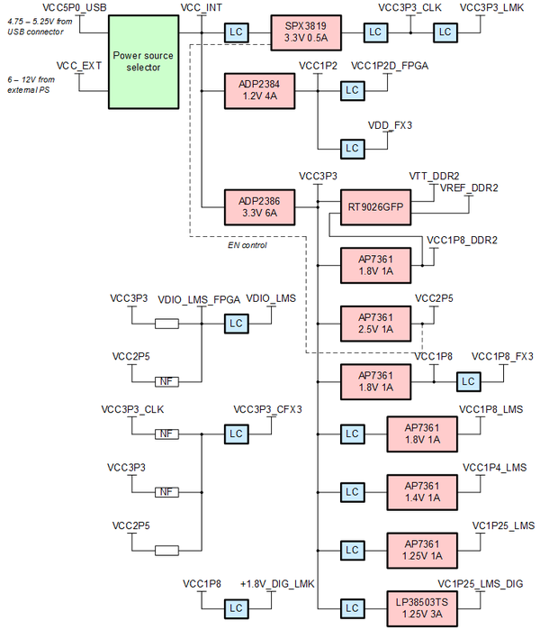
LimeSDR-USB board has complex power delivery network consisting of many different power rails with different voltages, filters, power sequences. LimeSDR-USB board power distribution block diagram is presented in Figure 13.
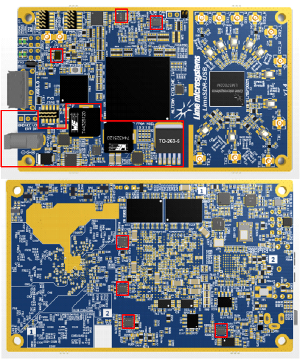
Power network power circuit ICs are presented in Figure 14.
| |||||||||||||||||||||