Zipper Interface Board Connections
Basic Connections
The Myriad-RF 1 board can be used as a stand-alone board or in conjunction with the Zipper board. The Myriad-RF 1 board is connected to the Zipper board via the standard connector FX10A-80P. For more information on standalone use, see Myriad-RF 1 Connections.
Zipper Interface Board Connections


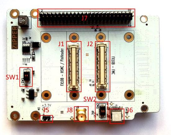
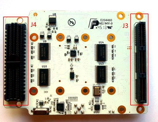
The following table describes the Zipper board connectors:
| Connector | Name | Description |
|---|---|---|
| J1 | Myriad-RF 1 to HSMC and Pin Header | Connects the Myriad-RF 1 board with HSMC and the Pin Header via the FX10A-80P standard connector. |
| J2 | Myriad-RF 1 to FMC and Pin Header | Connects the Myriad-RF 1 board with the FMC via the FX10A-80P standard connector. |
| J3 | HSMC | HSMC, standard Altera development kit connector, connected to all Myriad-RF 1 digital inputs and outputs. |
| J4 | FMC | FMC, standard Xilinx development kit connector, connected to all Myriad-RF 1 digital inputs and outputs. |
| J5 | +5 V | +5 V input power connector. |
| J6 | Mini-USB | USB connector. Provides +5 V supply for the Atmel microcontroller. |
| J7 | Pin Header | All Myriad-RF 1 inputs/outputs are connected. |
| J8 | SMA | Reference clock input for ADF4002 to lock the external clock from test equipment with DigiRED board clock. |
| SW1 | +12 V | When this switch is enabled, the Zipper board as well as the Myriad RF-1 board can be powered from a +12 V supply via the +5 V regulator fitted on the board. |
| SW2 | MCU | A hard reset switch for the Atmel microcontroller unit. |
J1 and J2 - Digital I/O Connectors
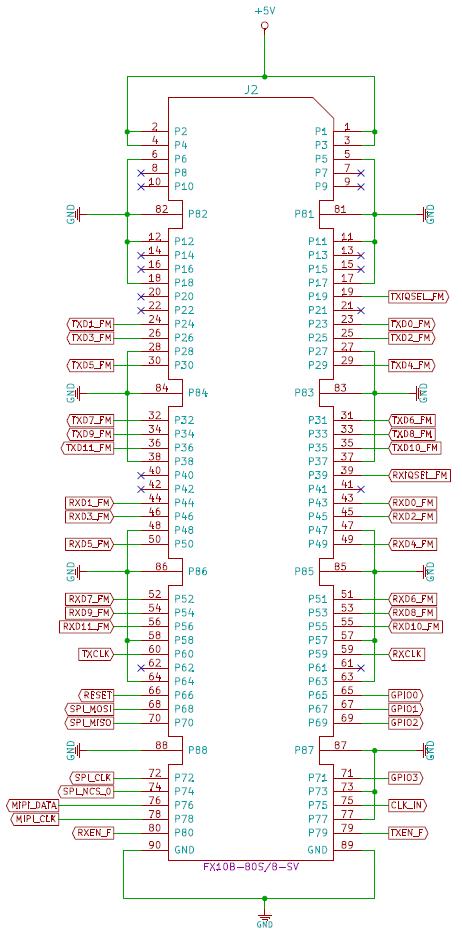
The Myriad-RF 1 board is directly plugged into one of the FX10A-80P type connectors. The digital I/O connector is a digital transmit (Tx) and receive (Rx) interface to the ADC/DAC of the LMS6002D. The SPI interface for the LMS6002D can also be established via the J1 and J2 connectors.

Hardware Options
The board is shipped in a default mode for basic operation. Various options are available depending on the system configuration required for testing or development work. The options are summarised below and the following sections describe the board modifications required to achieve these configurations.
Reference Frequency and Data Clocks Distribution
The Myriad-RF 1 provides a flexible clocking scheme which enables the PLL clock, RX clock and TX clock to be independently set. The Zipper board is shipped with a default mode using the on board 30.72 MHz clock for PLL clock only. The board can be reconfigured to allow users to provide clock frequency for digital interface and PLL clock using programmable clock generator from Silicon Labs (Si5356) which is capable of synthesising four independent frequencies. The device has four outputs connected to the LMS6002DFN PLL clock, RX data interface clock, TX data interface clock and to the J6 connector. In order to reprogram theLMS6002D PLL frequency from the default setting of 30.72 MHz, please change the components on the Zipper board as given in the table below. Please note that NF denotes that component is not fitted:
| Reference Clock Options | ||
|---|---|---|
| Component | Default Mode - PLL Clock set to 30.72 MHz | Programmable Mode - PLL Clock Can be Reprogrammed |
| R15 | 0 Ohm | NF |
| R24 | NF | 0 Ohm |
SPI Options
The Zipper board offers two options for the SPI, GPIO and MIPI RF communication with the Myriad-RF 1 board:
- Communication established via USB interface (default configuration).
- Communication established via J3, J4 or J7 connectors. In other words, from an external baseband.
In order to ensure stable communication for the desired option, the component changes on the Zipper board are given in the table below. Please note that NF denotes that the component is not fitted:
| SPI Options | ||||
|---|---|---|---|---|
| SPI Line | Components | SPI via USB | SPI via J2, J4, or J7 | Description |
| RESET | R60 | 0 Ohm | NF | |
| R24 | NF | 0 Ohm | ||
| SPI_MOSI | R62 | 0 Ohm | NF | |
| R55 | NF | 0 Ohm | ||
| SPI_MISO | R61 | 0 Ohm | NF | |
| R54 | NF | 0 Ohm | ||
| SPI_SCLK | R63 | 0 Ohm | NF | |
| R56 | NF | 0 Ohm | ||
| SPI_NCS_0 | R64 | 0 Ohm | NF | |
| R47 | NF | 0 Ohm | ||
| SPI_NCS_1 | R59 | 0 Ohm | NF | Master enable for ADF4002 SPI interface. |
| R53 | NF | 0 Ohm | ||
| SPI_NCS_2 | R58 | 0 Ohm | NF | Master enable for Si5351 SPI interface. |
| R52 | NF | 0 Ohm | ||
| rowspan="2"GPIO 0 | R68 | 0 Ohm | NF | GPIO for RF switch, controlled via GUI. |
| R71 | NF | 0 Ohm | ||
| GPIO 1 | R69 | 0 Ohm | NF | GPIO for RF switch, controlled via GUI. |
| R72 | NF | 0 Ohm | ||
| rowspan="2"GPIO 2 | R70 | 0 Ohm | NF | GPIO for RF switch, controlled via GUI. |
| R73 | NF | 0 Ohm | ||
| GPIO 3 | R80 | 0 Ohm | NF | GPIO for RF switch, controlled via GUI. |
| R90 | NF | 0 Ohm | ||
| MIPI_DATA | R79 | 0 Ohm | NF | MIPI RF devices controlled via GUI. |
| R39 | NF | 0 Ohm | ||
| MIPI_CLK | R78 | 0 Ohm | NF | MIPI RF devices controlled via GUI. |
GPIO Control Truth Table
The RF switches on the Myriad-RF 1 board are controlled via the GPIO 0-3 logic signals. This enables the user to choose RF input/output depending on the operational frequency. The truth table of the GPIO 0-2 settings is shown below:
| LMS6002D RF Input/Output | GPIO0 | GPIO1 | GPIO2 | GPIO3 | Description |
|---|---|---|---|---|---|
| TX Out 1 | X | X | 0 | X | High band output (1500 - 3800 MHz) |
| TX Out 2 | X | X | 1 | X | Broadband output |
| RX In 1 | 1 | 1 | X | 0 | Low band input (300 - 2200 MHz) |
| RX In 2 | 0 | 1 | X | 0 | High band input (1500 - 3800 MHz) |
| RX In 3 | 0 | 0 | X | 0 | Broadband input |
| |||||||||||||||||||||