STREAM OpenRISC
About
The Stream OpenRISC SoC is a complete System on Chip running on the FPGA on the STREAM board. Its main usage is to control all the on-board peripheral devices and to provide a standalone platform for software defined radio applications. With the supplied Linux image, the SoC is capable of:
- Generating I/Q data in software to send to a MyriadRF board
- Receiving I/Q samples that can be processed with the on-chip OpenRISC CPU or forwaded to the USB3 interface
- Connect to a network with Ethernet
- Handle user I/O with a UART
For special purpose applications, the Linux image can be replaced with a light-weight real-time operating system (RTOS) or a custom bare-metal application to increase performance and real-time capabilities.
Specification
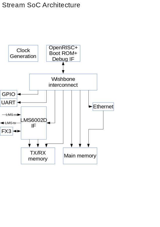
The Stream OpenRISC SoC consists of an OpenRISC CPU connected to various peripheral devices.
Block diagram

Stream SoC memory map
| Core | Base Address |
|---|---|
| Main Memory | 0x00000000 |
| TX/RX Memory | 0x04000000 |
| UART | 0x90000000 |
| GPIO | 0x91000000 |
| Ethernet MAC | 0x92000000 |
| LMS 6002D IF | 0x95000000 |
| Boot ROM | 0xF0000100 |
Boot ROM
The boot ROM contains the first instructions that the OpenRISC CPU will read after reset. The default behaviour is to clear register r3 and jump to address 0x100 and continue to load an application from there.
CPU
The OpenRISC Stream SoC uses mor1kx as main CPU.
Ethernet MAC
The 10/100 Mbps Ethernet MAC is used for Ethernet communication.
FX3
The FX3 interface is used for streaming received I/Q data to the on-board FX3 USB3 controller. The FX3 core implements a simple interface for writing to a synchronous slave interface of a Cypress FX3. Most parameters are fixed except for a input flag to signal flow control from the FX3 and data and write enable outputs to the FX3. The internal user interface consists of a 16-bit stream port.
| Name | Width | Direction | Comment |
|---|---|---|---|
| fd_0 | 16 | Out | Data to write to FX3 |
| slwr_n | 1 | Out | Active low write to enable FX3 |
| flagb | 1 | in | Flow control flag from FX3 to signal busy |
The FX3 interface should be connected directly to pins interfacing the FX3.
| Name | Width | Direction | Comment |
|---|---|---|---|
| stream_s_data_i | 16 | In | Internal data port |
| stream_s_valid_i | 1 | In | Internal data valid |
| stream_s_read_0 | 1 | Out | FX3 core is ready to accept data |
The Stream interface provides a port for providing data to the FX3 core. A successful transaction of a word occurs when both the valid and ready signals are asserted. This interface is synchronous to clk.
GPIO
The GPIO block is connected to the remaining FPGA_GPIO pins not used by UART. All pins can be programmed as either input or output separately.
| Bit | Onboard Pin |
|---|---|
| 0 | N.C. |
| 1 | N.C. |
| 2 | FPGA_GPIO2 |
| 3 | FPGA_GPIO3 |
| 4 | FPGA_GPIO4 |
| 5 | FPGA_GPIO5 |
| 6 | FPGA_GPIO6 |
| 7 | N.C. |
More documentation is available on the GitHub page.
Main Memory
The Main Memory controller is connected to 64MB DDR2 SDRAM. This memory is used for instructions and data for applications and operating systems.
TX/RX Memory
The TX/RX Memory controller is connected to 64MB DDR2 SDRAM. This memory is used for storing I/Q samples that are received , or to be transmitted from/to the LMS controller.
Myriad-RF Interface
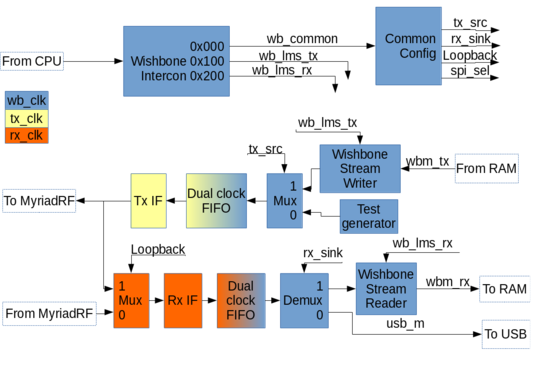
The Myriad-RF Interface, also known as the LMS6002D IF, is responsible for communication with a Myriad-RF 1 board. The external interface consists of an RX interface and a TX interface and the internal interfaces consist of two Wishbone master interfaces for streaming I/Q data to and from RAM, a Wishbone slave interface for control of Myriad-RF IF and a stream port for accessing the received data stream directly.
Block diagram

Interfaces
| Name | Width | Direction | Comment |
|---|---|---|---|
| txd | 12 | Out | TX I/Q Data from Myriad-RF 1 |
| txiqsel | 1 | Out | TX I/Q selector from Myriad-RF 1 |
| tx_clk | 1 | In | TX Clock from Myriad-RF 1 |
| tx_rst | 1 | In | Reset signal synchronous to tx_clk |
The TX interface should be connected directly to pins interfacing the MyriadRF, except for tx_rst which should be synchronized internally.
| Name | Width | Direction | Comment |
|---|---|---|---|
| rxd | 12 | In | RX I/Q Data from Myriad-RF 1 |
| rxiqsel | 1 | In | RX I/Q selector from Myriad-RF 1 |
| rx_clk | 1 | In | RX Clock from Myriad-RF 1 |
| rx_rst | 1 | In | Reset signal synchronous to rx_clk |
The RX interface should be connected directly to pins interfacing the Myriad-RF 1, except for rx_rst which should be synchronized internally.
| Name | Width | Direction | Comment |
|---|---|---|---|
| usb_m_data_0 | 24 | Out | RX I/Q Data from Myriad-RF 1. I=bits[23:12], Q=bits[11:0] |
| usb_m_valid_0 | 1 | Out | RX I/Q Data valid |
| usb_m_ready_i | 1 | In | Receiver ready |
The RX Stream interface provides a port for directly reading out the data stream from Myriad-RF 1. A successful transaction of a word occurs when both the valid and ready signals are asserted. This interface is synchronous to wb_clk.
| Name | Width | Direction | Comment |
|---|---|---|---|
| wbs_* | - | - | Wishbone slave interface for controlling the Myriad-RF IF core |
| wbm_tx_* | - | - | Wishbone master interface for reading TX samples from RAM |
| lms_tx_irq_0 | 1 | Out | Interrupt signal for TX DMA streamer |
| wbm_rx_* | - | - | RX DMA interface for writing received samples to RAM |
| lms_rx_irq_0 | 1 | Out | Interrupt signal for RX DMA streamer |
The Wishbone slave interface is used for control and status of the MyriadRF core. The memory map is detailed below.
| Register | Address | Comment |
|---|---|---|
| tx_src | 0x0000 | Source for TX I/Q Data. 0=Test data generator, 1=TX DMA streamer |
| loopback | 0x0008 | 0=Read I/Q sample from Myriad-RF 1, 1=Loop TX samples to RX |
| rx_sink | 0x000C | 0=Send RX data to Stream port, 1=Send RX data to RX DMA streamer |
| TX DMA | ||
| ctrl | 0x0100 | Bit 1=Interrupt, Bit 0=Streamer is busy |
| start_aadr | 0x0104 | Start address for reading samples in memory |
| buf_size | 0x0108 | Size of buffer to read from memory |
| burst_size | 0x010C | Length of Wishbone burst cycles |
| tx_cnt | 0x0110 | Number of bytes read for current transaction |
| RX DMA | ||
| ctrl | 0x0200 | Bit 1=Interrupt, Bit 0=Streamer is busy |
| start_adr | 0x0204 | Start address for writing samples in memory |
| buf_size | 0x0208 | Size of buffer to write to memory |
| burst_size | 0x020C | Length of Wishbone burst cycles |
| tx_cnt | 0x0210 | Number of bytes written for current transaction |
UART
The UART is used for standard input/output for software running on the SoC. The following pins are connected to the UART:
| Pin | Usage |
|---|---|
| FPGA_GPIO0 | TX (from computer to Stream board) |
| FPGA_GPIO1 | RX (from Stream board to computer) |
More documentation is available from OpenCores.org.
SoC Project Structure
- stream.system
- FuseSoC System configuration file
- stream.core
- FuseSoC core configuration file
- doc
- Documentation
- Makefile - Makefile to regenerate HTML docs
- \*.txt - AsciiDoc sources
- \*.html - HTML Documentation
- Documentation
- data
- Miscellaneous files
- stream.dts - Device Tree Source file
- stream.sdc - Timing constraints
- stream_defconfig - Linux default configuration
- pinmap.tcl - Pin mapping and I/O configuration
- wb_intercon_dbg.conf - Interconnect configuration file for mor1kx_dbg_wrapper
- options.tcl - Additional options for Quartus II
- winbond_w9751g6kb25.xml - Memory preset file for on-board DDR2 memories
- wb_intercon.conf - Configuration file for main Wishbone interconnect
- Miscellaneous files
- rtl/verilog
- SoC-specific verilog source code
- mor1kx_dbg_wrapper.v - Wrapper file for CPU, debug system and boot ROM
- rst_sync.v - Reset synchroniser
- include/timescale.v - Default verilog timescale setting
- include/uart_defines.v - UART default settings
- include/ethmac_defines.v - Ethernet MAC default settings
- stream_top.v - Stream SoC top-level
- wb_intercon.v - Main Wishbone Interconnect
- wb_intercon.vh - Main Wishbone Interconnect include file
- wb_intercon_dbg.v - mor1kx_dbg Wishbone Interconnect
- wb_intercon_dbg.vh - mor1kx_dbg Wishbone Interconnect include file
- altmemphy_wrapper.v - Wrapper for memory controller and arbiter
- clkgen.v - Clock generation
- SoC-specific verilog source code
- bench
- Testbench
- stream_tb.v - Stream SoC testbench wrapper
- test-defines.v - Test defines file
- Testbench
- ip
- Proprietary IP cores
- pll - Main PLL
- ddr2_ctrl - Altera Altmemphy DDR2 Controller
- Proprietary IP cores
See also
| |||||||||||||||||||||