LimeMicro:LMS6002D Datasheet: Difference between revisions
Ghalfacree (talk | contribs) m (Clarification of bandwidth.) |
Ghalfacree (talk | contribs) (Added additional applications.) |
||
| Line 17: | Line 17: | ||
* Femtocell and Picocell base stations | * Femtocell and Picocell base stations | ||
* Repeaters | * Repeaters | ||
* Broadband wireless communication devices for WCDMA/HSPA, LTE, GSM, CDMA2000, IEEE® 802.16x radios | * Broadband wireless communication devices for WCDMA/HSPA, LTE, GSM, CDMA2000, IEEE® 802.16x, Wi-Fi-(802.11) radios | ||
* Global Positioning System (GPS) | |||
* Digital Radio | |||
* Digital TV | |||
==Functional Block Diagram== | ==Functional Block Diagram== | ||
Revision as of 14:22, 23 September 2015
Summary
The Lime Microsystems LMS6002D is a multi-band, multi-standard transceiver with integrated dual digital to analogue (DAC) and analogue to digital (ADC) converters.
Features
- Single chip transceiver covering 0.3-3.8GHz frequency range
- Digital interface to baseband with integrated 12 bit D/A and A/D converters
- Fully differential baseband signals
- Few external components
- Programmable modulation bandwidth (RF): 1.5, 1.75, 2.5, 2.75, 3, 3.84, 5, 5.5, 6, 7, 8.75, 10, 12, 14, 20 and 28MHz
- Supports both TDD and FDD operation modes
- Low voltage operation, 1.8V and 3.3V
- 120-pin DQFN package
- Power down option
- Serial port interface
Applications
- Femtocell and Picocell base stations
- Repeaters
- Broadband wireless communication devices for WCDMA/HSPA, LTE, GSM, CDMA2000, IEEE® 802.16x, Wi-Fi-(802.11) radios
- Global Positioning System (GPS)
- Digital Radio
- Digital TV
Functional Block Diagram
General Description
The LMS6002D is a fully integrated, multi-band, multi-standard RF transceiver for 3GPP (WCDMA/HSPA, LTE), 3GPP2 (CDMA2000) and 4G LTE applications, as well as for GSM pico BTS. It combines the LNA, PA driver, RX/TX mixers, RX/TX filters, synthesizers, RX gain control, and TX power control with very few external components.
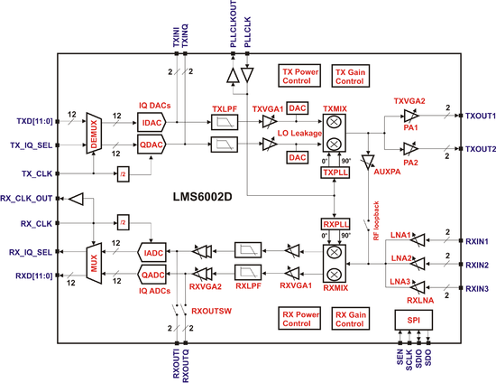
The top level architecture of LMS6002D transceiver is shown in the functional block diagram. Both transmitter and receiver are implemented as zero IF architectures providing up to 28MHz modulation bandwidth (equivalent to 14MHz baseband IQ bandwidth).
On the transmit side, IQ DAC samples from the baseband processor are provided to the LMS6002D on a 12 bit multiplexed parallel CMOS input level bus. Analogue IQ signals are generated by on chip transmit DACs. These are fed to the TXINI and TXINQ inputs. Transmit low pass filters (TXLPF) remove the images generated by zero hold effect of the DACs. The IQ signals are then amplified (TXVGA1) and DC offset is inserted in the IQ path by LO leakage DACs in order to cancel the LO leakage. The IQ signals are then mixed with the transmit PLL (TXPLL) output to produce a modulated RF signal. This RF signal is then split and amplified by two separate variable gain amplifiers (TXVGA2) and two off chip outputs are provided as RF output.
Transmitter gain control range of 56dB is provided by IF (TXVGA1, 31dB range) and RF (TXVGA2, 25 dB range) variable gain amplifiers. Both TXVGAs have 1dB gain step control.
The LMS6002D provides an RF loop back option (see the functional block diagram) which enables the TX RF signal to be fed back into the baseband for calibration and test purposes. The RF loop back signal is amplified by an auxiliary PA (AUXPA) in order to increase the dynamic range of the loop.
On the receive side, three separate inputs are provided each with a dedicated LNA. Each port preconditioned RF signal is first amplified by a programmable low noise amplifier (RXLNA). The RF signal is then mixed with the receive PLL (RXPLL) output to directly down convert to baseband. Large AGC steps can be implemented by an IF amplifier (RXVGA1) prior to the programmable bandwidth lowpass channel select filters (RXLPF). The received IQ signal is further amplified by a programmable gain amplifier RXVGA2. DC offset is applied at the input of RXVGA2 to prevent saturation and to preserve receive the ADC(s) dynamic range. The resulting analogue receive IQ signals are converted into the digital domain using the on chip receive ADCs and provided as an output to the baseband processor on a multiplexed 12 bit CMOS output level parallel bus. The receive clock, RX_CLK, is provided off chip at the RX_CLK_OUT pin and can be used to synchronise with the baseband digital receive data sampling clock.
By closing the RXOUT switch and powering down RXVGA2, the RXOUTI and RXOUTQ pins can be used as IQ ADCs inputs. In this configuration the ADCs can be used to measure two external signals, such as an off chip PA temperature sensor or peak detector.
Two transmitter outputs (TXOUT1, TXOUT2) and three receiver inputs (RXIN1, RXIN2, RXIN3) are provided to facilitate multi-band operation.
The functionality of the LMS6002D is fully controlled by a set of internal registers which can be accessed through a serial port.
In order to enable full duplex operation, the LMS6002D contains two separate synthesisers (TXPLL, RXPLL) both driven from the same reference clock source PLLCLK. The PLLCLK signal is provided at the PLLCLKOUT output pin and can be used as the baseband clock.
Differential signalling is done in the receive and transmit analogue paths throughout the chip.
Specifications
General Specifications
| Parameter | Condition/Comment | Min | Typ | Max | Unit |
|---|---|---|---|---|---|
| TRX RF Frequency Range | 0.3 | 3.8 | GHz | ||
| Baseband Bandwidth | 0.75 | 14 | MHz | ||
| Frequency Resolution | Using 41MHz PLL reference clock | 2.4 | Hz | ||
| TRX 3.3V Supply | 3.1 | 3.3 | 3.5 | V | |
| TRX 1.8V Supply | 1.7 | 1.8 | 1.9 | V | |
| TX Supply Current | At maximum gain | 280 | mA | ||
| RX Supply Current | At maximum gain | 220 | mA | ||
| Digital Core Supply Voltage | 1.7 | 1.8 | 1.9 | V | |
| Digital Peripheral (IO) Supply Voltage | Can go below 3.3V nominal to support LV CMOS signalling | 1.7 | 3.3 | 3.5 | V |
| Ambient Temperature | -40 | 25 | 85 | °C | |
| Storage Temperature | -65 | 125 | °C | ||
| Maximum RF Output Power | Continuous wave | 6 | dBm | ||
| Absolute Maximum RF Input Power | No damage | 23 | dBm | ||
| PLL Reference Clock | For continuous LO frequency range | 23 | 41 | MHz | |
| PLL Phase Noise | 1MHz offset | -125 | dBc/Hz |
RF Specifications
| Parameter | Condition/Comment | Min | Typ | Max | Unit |
|---|---|---|---|---|---|
| TRX RF Bandwidth | 0.3 | 3.8 | GHz | ||
| Transmit Input Impedance | Differential, programmable | 100 | Ohms | ||
| Transmit Load Impedance | Differential | 65 | Ohms | ||
| Transmit Differential I and Q Input Voltages | Differential | 250 | mVpp | ||
| Common mode | 65 | mV | |||
| Transmit Gain Control Range | TXVGA1, TXVGA2 | 56 | dB | ||
| Transmit Gain Control Step | 1 | dB | |||
| TX LO Leakage | LO leakage not calibrated | -50 | dBc | ||
| RX LNA1 Frequency Range | Narrow band | 0.3 | 2.8 | GHz | |
| RX LNA2 Frequency Range | Narrow band | 1.5 | 3.8 | GHz | |
| RX LNA3 Frequency Range | Broad band | 0.3 | 3.8 | GHz | |
| RX LNA1 Input Impedance | Differential | 50 | Ohms | ||
| RX LNA2 Input Impedance | Differential | 50 | Ohms | ||
| RX LNA3 Input Impedance | Differential | 200 | Ohms | ||
| Receive Load Impedance | Differential | 2K | Ohms | ||
| Receive Load Capacitance | 5 | pF | |||
| Noise Figure | LNA1 at 0.95GHz | 3.5 | dB | ||
| LNA2 at 1.95GHz | 5.5 | ||||
| LNA3 at 1.95GHz | 10 | ||||
| 3rd Order Input Referred Intercept Point | LNA2 at Mid. Gain | -1 | dBm | ||
| Receive Gain Control Range | RXLNA, RXVGA1, RXVGA2 | 61 | dBm | ||
| Receive Gain Control Step | RXVGA1, not log-linear | 1 | dB | ||
| RXVGA2 | 3 |
Gain Control
TX Gain Control
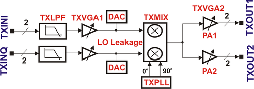
The LMS6002D transmitter has two programmable gain stages: TXVGA1, located in the IF section; and TXVGA2, in the RF section. TXVGA1 is implemented on the I and Q branches but controlled by a single control word. TXVGA2 consists of 2 amplifiers one for each of the transmitter outputs, however only one of these output amplifiers can be active at any time.
Note: The TXLPF has a gain of 6dB or 0dB when bypassed.
| Parameter | Condition | Min | Typ | Max | Unit |
|---|---|---|---|---|---|
| TXLPF Gain | 0dB gain when bypassed | 0 | 6 | dB | |
| TXVGA1 Gain Control Range | 31 | dB | |||
| TXVGA1 Gain Step Size | Guaranteed monotonic | 1 | dB | ||
| TXVGA2 Gain Control Range | 25 | dB | |||
| TXVGA2 Gain Step Size | Guaranteed monotonic | 1 | dB |
RX Gain Control
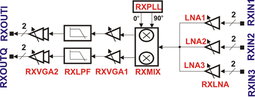
The LMS6002D receiver has three gain control elements: RXLNA, RXVGA1, and RXVGA2. RXLNA gain control consists of a single 6dB step for AGC when large in co-channel blockers are present and a reduction in system NF is acceptable. The main LNAs (LNA1 and LNA2) have fine gain control via a 6 bit word which offers ±6dB control intended for frequency correction when large input bandwidths are required.
RXVGA1 offers 25dB of control range. A 7 bit control word is used and the response is not log-linear. Maximum step size is 1dB. RXVGA1 is intended for AGC steps needed to reduce system gain prior to the channel filters when large in band blockers are present. This gain can be under control of the baseband or fixed on calibration.
RXVGA2 provides the bulk of gain control for AGC if a constant RX signal level at the ADC input is required. It has 30dB gain range control in 3dB steps.
Note: RXLPF has a gain of 0dB when bypassed.
| Parameter | Condition | Min | Typ | Max | Unit |
|---|---|---|---|---|---|
| RXLNA Gain Control Range | Single step | 0 | 6 | dB | |
| RXVGA1 Gain Control Range | 25 | dB | |||
| RXVGA1 Gain Step Size | Not log-linear | 1 | dB | ||
| RXLPF Gain | 0dB gain when bypassed | 0 | 6 | dB | |
| RXVGA2 Gain Control Range | 30 | dB | |||
| RXVGA2 Gain Step Size | Guaranteed monotonic | 3 | dB |
Synthesisers
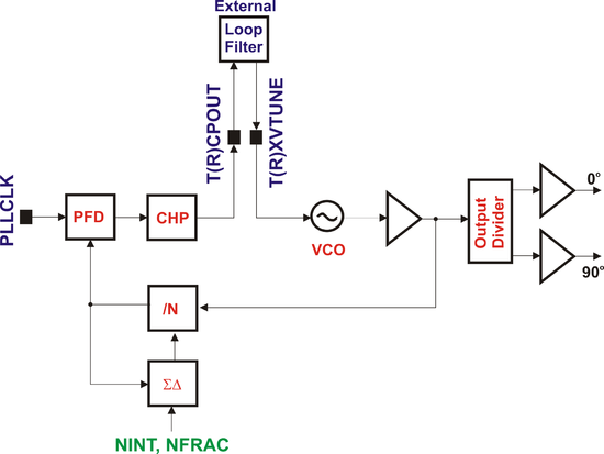
The LMS6002D has two low phase noise synthesisers to enable full duplex operation. Both synthesisers are capable of output frequencies up to 3.8GHz. Each synthesiser uses a fractional-N PLL architecture. The same reference frequency is used for both synthesisers and is flexible between 23 to 41MHz. The synthesisers produce a complex output with suitable level to drive IQ mixers in both the TX and the RX paths.
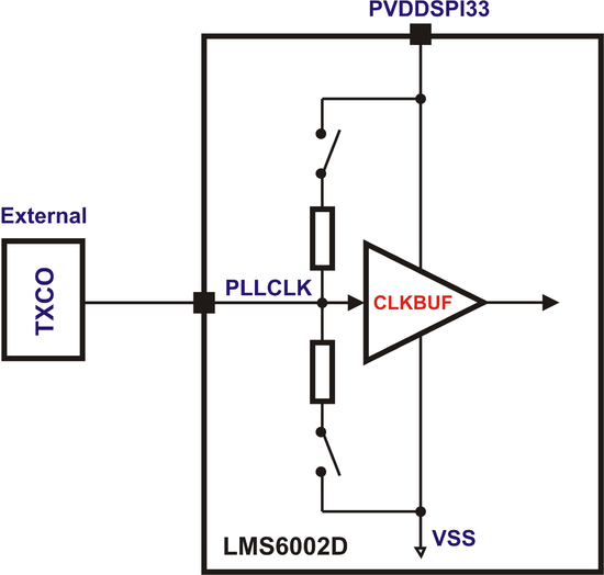
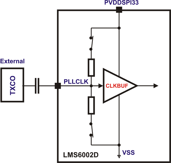
The LMS6002D can accept clipped sine as well as the CMOS level signals as the PLL reference clock. Both DC and [#AC Coupled|AC]] coupling are supported. Internal buffer self biasing must be enabled for AC coupling mode. PLL reference clock input can also be low voltage CMOS (2.5V or 1.8V, for example) which is implemented by lowering clock buffer supply PVDDSPI33.
| Parameter | Condition | Min | Typ | Max | Unit |
|---|---|---|---|---|---|
| Frequency Range | 0.3 | 3.8 | GHz | ||
| Reference Amplitude | At PVDDSPI33=3.3V | 0.2 | 0.8 | 3.3 | Vpp |
| Reference Frequency | For continuous LO frequency range | 23 | 41 | MHz | |
| Frequency Step Size | At 41MHz reference clock | 2.4 | Hz | ||
| Phase Noise | 800MHz | dBc/Hz | |||
| 10KHz offset | -94 | ||||
| 100KHz offset | -113 | ||||
| 1MHz offset | -130 | ||||
| Phase Noise | 1.9GHz | ||||
| 10KHz offset | -89 | ||||
| 100KHz offset | -95 | ||||
| 1MHz offset | -125 | ||||
| Phase Noise | 2.6GHz | ||||
| 10KHz offset | -86 | ||||
| 100KHz offset | -90 | ||||
| 1MHz offset | -125 | ||||
| Reference Spurious Outputs | -50 | dBc | |||
| Other Spurious Outputs | -50 | dBc | |||
| IQ Phase Error | 800MHz | 1 | deg | ||
| 1.9GHz | 3 | ||||
| 2.6GHz | 9 | ||||
| IQ Amplitude Error | 0.4 | dB | |||
| PLL Settling Time | To 1ppm, 50KHz loop bandwidth | 20 | μs |
DC Coupled
AC Coupled
RF Ports
The LMS6002D has two transmitter outputs and three receiver inputs.
The transmitter output ports are optimized for a 65Ω differential load, the final stage amplifiers are open drain and require +3.3V voltage supply, see LMS6002D typical application circuit in the typical application circuit.
The receiver inputs are all different: RXIN1 is the low frequency input and can operate in the range 0.3 – 2.8GHz; RXIN2 is the high frequency input and can operate in the range 1.5 – 3.8GHz. Both RXIN1 and RXIN2 require matching circuits for optimum performance. A simple match is shown in the typical application circuit. RXIN3 is a broadband input covering the range 0.3 – 3.0GHz, it is 200Ω differential and is typically matched with a wideband transformer.
TX and RX Low Pass Filters
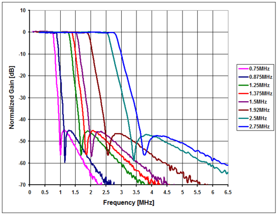
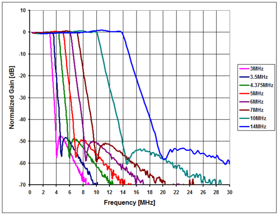
The LMS6002D integrates highly selective low pass filters in both TX and RX paths. Filters have a programmable pass band in order to provide more flexibility on the DAC/ADC clock frequency and also to provide excellent adjacent channel rejection in the receive chain. The following LPF pass bands are supported: 14, 10, 7, 6, 5, 4.375, 3.5, 3, 2.75, 2.5, 1.92, 1.5, 1.375, 1.25, 0.875, and 0.75MHz. Filters are also tunable to compensate for process/temperature variation. The TX and RX filters are the same but controlled via SPI link independently. Measured amplitude responses are shown in Amplitude Response.
Assuming 40MHz DAC/ADC clock, 28MHz modulation bandwidth (equivalent to 14MHz baseband IQ bandwidth) and 28MHz channel spacing, performance of the TRX filters is summarised as below.
TX Low Pass Filter Performance
- First DAC image attenuation >= 55dB
- Second DAC image attenuation >= 70dB
RX Low Pass Filter Performance
- Alias attenuation >= 50dB
- First adjacent channel attenuation >= 45 dB
- Second adjacent channel attenuation >= 70 dB
Amplitude Response
Calibration and Initialisation
There are a number of calibrations which the LMS6002D can carry out internally when instructed via the SPI. These calibrations can be initiated on power up/reset to produce optimum settings. The following auto calibration options are available:
- DC offset cancellation within the various blocks
- TRX LPF bandwidth tuning
Additionally, LMS6002D provides the blocks such as LO leakage DACs and RF loop back to further facilitate the following calibrations:
- LO leakage in the transmit chain
- IQ gain and phase mismatch in both transmit and receive chains
Note that these calibrations require the loop to be closed externally via the baseband.
Recommended Initialisation Sequence
- Apply RESET pulse (active low). This sets all the configuration registers to their default values.
- Set target LO frequency and gain for both TX and RX chains.
- LPF tuning.
- DC offset cancellation of the tuning module
- Execute LPF bandwidth tuning procedure
- TXLPF
- DC offset cancellation of I filter
- DC offset cancellation of Q filter
- RXLPF
- DC offset cancellation of I filter
- DC offset cancellation of Q filter
- RXVGA2
- DC offset cancellation of the reference generator
- DC offset cancellation of the first gain stage, I branch
- DC offset cancellation of the first gain stage, Q branch
- DC offset cancellation of the second gain stage, I branch
- DC offset cancellation of the second gain stage, Q branch
- TX LO leakage cancellation
- TX IQ gain/phase error calibration
- RX IQ gain/phase error calibration
Once the device is calibrated, register values can be stored and uploaded back into LMS6002D at the next power up/reset point which will shorten the initialisation time. Refer to the LMS6002D Programming and Calibration Guide for more details.
Digital IQ Data Interface
Description
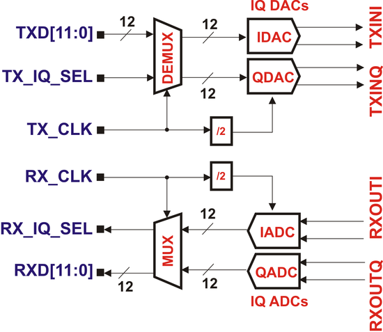
The functionality of LMS6002D transceiver implements a subset of the LimeLight LMS600X-01008031 digital IQ interface with a 12 bit multiplexed transmit path and a 12 bit multiplexed receive path. TX and RX interfaces require a clock running at twice the data converters sample rate. Separate clocks can be provided for the TX and RX interface. Location of the IQ samples in the multiplexed stream is flagged by the IQ select signals which are required as an input to the transmit path and provided as an output from the receive path.
Frame Sync Polarity and Interleave Modes
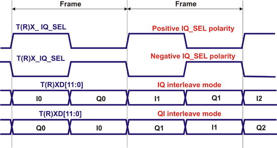
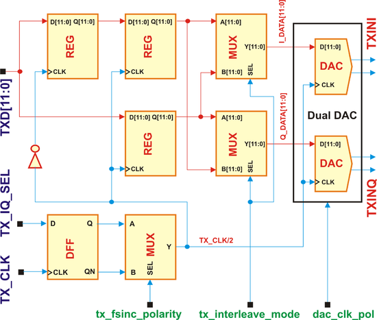
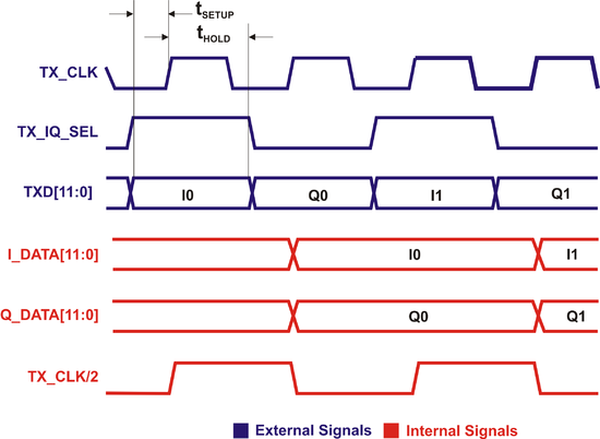
For both TX and RX interfaces IQ_SEL (frame sync) polarity and interleave mode are independently programmable via the SPI link. Here, the frame is defined as two consecutive T(R)X_CLK, i.e. one T(R)X_IQ_SEL, periods while IQ data from the same sampling point are present on the multiplexed bus.
Transmitter Data Interface
A more detailed functional diagram of the TX data interface is shown above alongside corresponding waveforms. The interface is a 12 bit parallel bus from the base band IC carrying multiplexed IQ data samples for the transmit DACs. The interface data rate is twice the DACs sample rate. TX_IQ_SEL flag is used to identify I and Q samples on the multiplexed bus. Note that the DACs sampling clock is not derived by dividing TX_CLK by two as indicated in Frame Sync Polarity and Interleave Modes. Instead, registered version of TX_IQ_SEL is used. Hence, for the DACs to receive sampling clock TX_IQ_SEL must be provided and toggled as in Frame Sync Polarity and Interleave Modes. DACs sampling edge is also programmable via SPI link.
The TX digital IQ interface related pins are described as follows:
- TX_CLK
- TX interface data clock, positive edge sensitive (input)
- TXD[11:0] - 12 bit multiplexed IQ data bus (input)
- TX_IQ_SEL Indicates the location of I and Q data on the multiplexed bus (input)
Some examples of the TX interface data rates are provided below:
- DACs sample rate
- WCDMA 15.36 MS/s
- GSM 1.083 MS/s
- TX IQ interface data rate
- WCDMA 30.72 MS/s
- GSM 2.167 MS/s
Receiver Data Interface
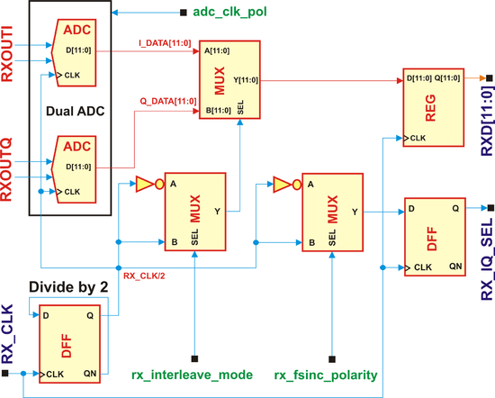
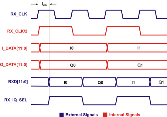
A more detailed functional diagram of the RX data interface is shown above, alongside corresponding waveforms. The interface is a 12 bit parallel bus output from the LMS6002D to the base band IC carrying multiplexed IQ data samples from the receive ADCs. The interface data rate is twice the ADCs sample rate. RX_IQ_SEL flag is provided to identify I and Q samples on the multiplexed bus. The receive clock coming from the baseband is on chip divided by two before being used by the ADC’s. The ADCs sampling edge is also programmable via SPI link.
RX digital IQ interface related pins are described as follows:
- RX_CLK
- RX interface data clock, positive edge sensitive (input)
- RXD[11:0]
- 12 bit multiplexed IQ data bus (output)
- RX_IQ_SEL
- Indicates the location of I and Q data on the multiplexed bus (output)
Some examples of the RX interface data rates are provided below:
- ADCs sample rate
- WCDMA 15.36 MS/s
- GSM 1.083 MS/s
- RX IQ interface data rate
- WCDMA 30.72 MS/s
- GSM 2.167 MS/s
IQ Interface Timing Parameters
| Parameter | Min | Typ | Max | Unit |
|---|---|---|---|---|
| TX Setup Time (tSETUP) | 1 | ns | ||
| TX Hold Time (tHOLD) | 0.2 | ns | ||
| RX Output Delay (tOD at 15pF Load | 6 | ns |
DACs Electrical Specifications
(At TA = 25°C, TAVDD33 = 3.3 V, FCLK = 40 MSPS, FOUT = 4 MHz, internal references, -1 dBFS input signal unless otherwise noted)
| Parameter | Condition | Min | Typ | Max | Unit |
|---|---|---|---|---|---|
| Digital Core Supply | 1.7 | 1.8 | 1.9 | V | |
| Analogue Supply | 3.1 | 3.3 | 3.5 | V | |
| Number of Bits | Two's Complement format | 12 | bits | ||
| DAC Sampling Rate | 40 | MHz | |||
| Full Scale Current | Programmable | 2.5 | mA | ||
| Output Amplitude | At 100 Ohm differential load | 250 | mVpp diff. | ||
| SFDR | 60 | dBc | |||
| ENOB | 10 | bits |
ADCs Electrical Specifications
(At TA = 25°C, RAVDD18 = 1.8 V, FCLK = 40 MSPS, FOUT = 4 MHz, internal references, -1 dBFS input signal unless otherwise noted)
| Parameter | Condition | Min | Typ | Max | Unit |
|---|---|---|---|---|---|
| Digital Core Supply | 1.7 | 1.8 | 1.9 | V | |
| Analogue Supply | 1.7 | 1.8 | 1.9 | V | |
| Number of Bits | Two's Complement format | 12 | bits | ||
| ADC Sampling Rate | 40 | MHz | |||
| Input Amplitude | Differential | 1 | 1.8 | Vpp | |
| Input Common Mode Voltage | Input buffer off | 0.9 | V | ||
| Input Impedance | 2 | kOhm | |||
| ENOB | 10 | bits |
Digital IQ Interface IO Buffers Specifications
| Parameter | Condition | Min | Typ | Max | Unit |
|---|---|---|---|---|---|
| Supply Voltage (PVDD) | Can go below 3.3V nominal to support LVCMOS signalling | 1.7 | 3.3 | 3.5 | V |
| Input High (VIH) | PVDD-0.8 | V | |||
| Input Low (VIL) | 0.8 | V | |||
| Output High (VOH) | PVDD-0.4 | V | |||
| Output Low (VOL) | 0.4 | V | |||
| Input Pad Capacitance (CIN) | 3.5 | pF | |||
| Output Drive Current1 | 8 | mA |
1 Maximum peak current that flows when the output digital lines change state and begin charging the load capacitance.
Implementing Low Voltage Digital IQ Interface
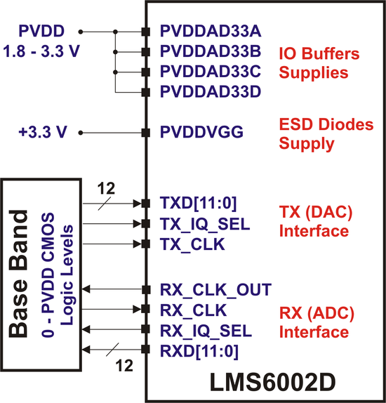
Digital IO buffers in LMS6002D are supplied using four pins (PVDDAD33A - PVDDAD33D). All these pins must be supplied by the same supply PVDD. There is one additional supply pin (PVDDVGG) dedicated for ESD protection diodes supply. PVDDVGG must be supplied by +3.3V. However, PVDD can go below 3.3V to implement low voltage signaling. For example, if PVDD=2.5V then all data lines in the above figure are set to 2.5V CMOS IOs. Having PVDDVGG=3.3V sets all inputs to be 3.3V tolerant. Minimum PVDD is 1.8V.
Serial Port Interface
Description
The functionality of LMS6002D transceiver is fully controlled by a set of internal registers which can be accessed through a serial port interface. Both write and read SPI operations are supported. The serial port can be configured to run in 3 or 4 wire mode with the following pins used:
- SEN
- serial port enable, active low
- SCLK
- serial clock, positive edge sensitive
- SDIO
- serial data in/out in 3 wire mode
- serial data input in 4 wire mode
- SDO
- serial data out in 4 wire mode
- don’t care in 3 wire mode
Serial port key features:
- 16 SPI clock cycles are required to complete write operation.
- 16 SPI clock cycles are required to complete read operation.
- Multiple write/read operations are possible without toggling serial port enable signal.
All configuration registers are 8-bit wide. Write/read sequence consists of 8-bit instruction followed by 8-bit data to write or read. MSB of the instruction bit stream is used as SPI command where CMD=1 for write and CMD=0 for read. Remaining 7 bits of the instruction represent register address.
The write/read cycle waveforms are reproduced below. Note that the write operation is the same for both 3-wire and 4-wire modes. Although not shown in the figures, multiple byte write/read is possible by repeating the instruction/data sequence while keeping SEN low.
Write Operation Waveform

Read Operation Waveform, 4-Wire (Default)

Read Operation Waveform, 3-Wire

SPI Memory Map
The LMS6002D configuration registers are divided into eight logical blocks. 3 MSBs of the available 7-bit address are used as block address while the remaining 4 bits are used to address particular registers within the block.
Integer and fractional part of the PLL divider are stored in four bytes of configuration memory. To change their values, four write cycles are required. Hence, the controlled PLL should see new NINT and NFRAC when all four bytes are updated, otherwise it will generate unpredicted and wrong LO frequency while being configured. Such parameters are provided through a shadow register. Shadow register outputs new values only when SEN is high, i.e. there is no access to configuration memory. For that reason, DSM (PLL) SPI synchronization clock, derived from the PLL reference, must be enabled while writing to or reading from the PLL configuration registers and should last at least two cycles more after SEN goes high.
| Address (7 bits) | Description |
|---|---|
| 000:xxxx | Top level configuration |
| 001:xxxx | TX PLL |
| 010:xxxx | RX PLL |
| 011:xxxx | TX LPF |
| 100:xxxx | TX RF |
| 101:xxxx | RX LPF, DACs and ADCs |
| 110:xxxx | RX VGA2 |
| 111:xxxx | RX RF |
Implementing Low Voltage SPI
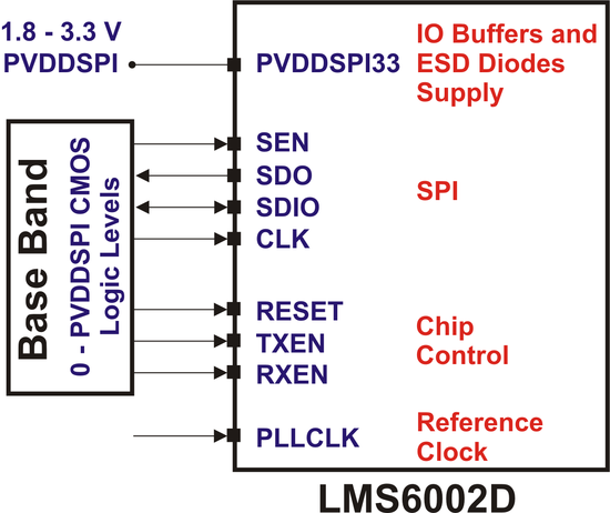
Digital IO buffers and ESD protection diodes in the SPI region are all supplied from a single pin PVDDSPI33. PVDDSPI33 can go below 3.3V to implement low voltage signaling. For example, if PVDDSPI33=2.5V then all data lines in the above figure, including PLL reference clock input, are set to 2.5V CMOS IOs. There is no dedicated ESD protection diodes supply here so when PVDDSPI33 is less than 3.3V, inputs will not be 3.3V tolerant. Minimum PVDDSPI33 is 1.8V.
Package Outline and Pin Description
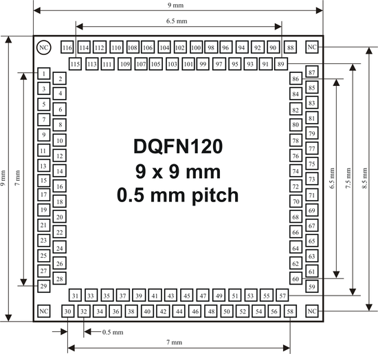
| Pin No. | Pin Name | Type | Description | Note |
|---|---|---|---|---|
| 1 | PVDDAD33A | pads supply | ADCs/DACs IOs supply (3.3V) | Can be lowered down to 1.8V to support LV signalling |
| 2 | RXD11 | out cmos | ADCs digital output, bit 11 (MSB) | Two's complement |
| 3 | RXD10 | out cmos | ADCs digital output, bit 10 | |
| 4 | RXD9 | out cmos | ADCs digital output, bit 9 | |
| 5 | RXD8 | out cmos | ADCs digital output, bit 8 | |
| 6 | RXD7 | out cmos | ADCs digital output, bit 7 | |
| 7 | PVDDVGG | esd supply | ADCs/DACs IOs ESD supply (3.3V) | |
| 8 | RXD5 | out cmos | ADCs digital output, bit 5 | |
| 9 | RXD6 | out cmos | ADCs digital output, bit 6 | |
| 10 | RXD3 | out cmos | ADCs digital output, bit 3 | |
| 11 | RXD4 | out cmos | ADCs digital output, bit 4 | |
| 12 | PVDDAD33B | pads supply | ADCs/DACs IOs supply (3.3V) | Can be lowered down to 1.8V to support LV signalling |
| 13 | RXD2 | out cmos | ADCs digital output, bit 2 | |
| 14 | RXD1 | out cmos | ADCs digital output, bit 1 | |
| 15 | RXD0 | out cmos | ADCs digital output, bit 0 (LSB) | |
| 16 | RX_IQ_SEL | out cmos | RX digital interface IQ flag | |
| 17 | RX_CLK | in cmos | RX digital interface clock | |
| 18 | PVDDAD33C | pads supply | ADCs/DACs IOs supply (3.3V) | Can be lowered down to 1.8V to support LV signalling |
| 19 | TX_CLK | in cmos | TX digital interface clock | |
| 20 | TX_IQ_SEL | in cmos | TX digital interface IQ flag | |
| 21 | TXD0 | in cmos | DACs digital input, bit 0 (LSB) | |
| 22 | TXD1 | in cmos | DACs digital input, bit 1 | |
| 23 | TXD2 | in cmos | DACs digital input, bit 2 | |
| 24 | TXD3 | in cmos | DACs digital input, bit 3 | |
| 25 | TXD4 | in cmos | DACs digital input, bit 4 | |
| 26 | TXD5 | in cmos | DACs digital input, bit 5 | |
| 27 | TXD6 | in cmos | DACs digital input, bit 6 | |
| 28 | TXD7 | in cmos | DACs digital input, bit 7 | |
| 29 | TXD8 | in cmos | DACs digital input, bit 8 | |
| 30 | TXD9 | in cmos | DACs digital input, bit 9 | |
| 31 | TXD10 | in cmos | DACs digital input, bit 10 | |
| 32 | TXD11 | in cmos | DACs digital input, bit 11 (MSB) | Two's complement |
| 33 | RDVDD18 | digital supply | ADCs digital supply (1.8V) | |
| 34 | PVDDAD33D | pads supply | ADCs/DACs pads supply (3.3V) | Can be lowered down to 1.8V to support LV signalling |
| 35 | RAVDD18 | analogue supply | ADCs analogue supply (1.8V) | |
| 36 | TDVDD18 | digital supply | DACs digital supply (1.8V) | |
| 37 | TAVDD33 | analogue supply | DACs analogue supply (3.3V) | |
| 38 | VREFAD | in/out | External capacitor for ADCs/DACs (>100nF) | |
| 39 | XRESAD | in/out | External resistor for ADCs/DACs | |
| 40 | RX_CLK_OUT | out cmos | Buffered RX_CLK (ADCs) clock, CMOS level | Can be used to align RXD[11:0] sampling clock in BB. |
| 41 | PLLCLKOUT | out cmos | Buffered PLLCLK (PLL reference) clock, CMOS level | Can be used as BB clock. |
| 42 | ATP | out | Analogue test point | |
| 43 | TXVCCLPF33 | analogue supply | TXLPF supply (3.3V) | |
| 44 | TXOUT2N | out | TX output 2, negative | |
| 45 | TXVCCMIX33 | analogue supply | TXMIX supply (3.3V) | |
| 46 | TXOUT2P | out | TX output 2, positive | |
| 47 | TXPVDD33 | esd supply | TX pads ESD supply (3.3V) | |
| 48 | TXOUT1P | out | TX output 1, positive | |
| 49 | TXVCCDRV33 | analogue supply | TXVGA2 supply (3.3V) | |
| 50 | TXOUT1N | out | TX output 1, negative | |
| 51 | TXININ | in/out | TXDAC output / TXLPF input | |
| 52 | TXINIP | in/out | TXDAC output / TXLPF input | |
| 53 | UNUSED | Connect to ground | ||
| 54 | TXINQP | in/out | TXDAC output / TXLPF input | |
| 55 | UNUSED | Connect to ground | ||
| 56 | TXINQN | in/out | TXDAC output / TXLPF input | |
| 57 | TXVTUNE | in/out | TXPLL loop filter output | |
| 58 | TXPVDDPLL33A | esd supply | TXPLL pads ESD supply (3.3V) | |
| 59 | TXVCCVCO33 | analogue supply | TXPLL 3.3V supply (3.3V) | |
| 60 | TXVDDVCO18 | analogue supply | TXPLL VCO supply (1.8V) | |
| 61 | TXVCCPLL18 | digital supply | TX PLL modules 1.8V supply (1.8V) | |
| 62 | TXPVDDPLL33B | esd supply | TX PLL pads ESD supply (3.3V) | |
| 63 | TXVCCCHP33 | analogue supply | TX PLL charge pump supply (3.3V) | |
| 64 | TXCPOUT | in/out | Transmit PLL loop filter input | |
| 65 | TSTD_out1 | out cmos | TX and RX PLLs digital test point | |
| 66 | TXEN | in cmos | Transmitter enable, active high | |
| 67 | SEN | in cmos | Serial port enable, active low | |
| 68 | SDO | out cmos | Serial port data out | High Z when SEN=1 |
| 69 | SDIO | in/out cmos | Serial port data in/out | |
| 70 | SCLK | in cmos | Serial port clock, positive edge sensitive | |
| 71 | PLLCLK | in, cmos or clipped sine | PLL reference clock input (23MHz - 41 MHz) | Minimum input level is 0.2Vpp. Both DC and AC coupling supported. |
| 72 | TRXVDDDSM18 | digital supply | Delta sigma digital core supply (1.8V) | |
| 73 | VSPI18 | digital supply | SPI digital core supply (1.8V) | |
| 74 | PVDDSPI33 | esd supply | SPI pads and ESD Supply (3.3V) | Can be lowered down to 1.8V to support LV signalling |
| 75 | RESET | in cmos | Hardware reset, active low | |
| 76 | RXEN | in cmos | Receiver enable, active high | |
| 77 | TSTD_out2 | out cmos | TX and RX PLLs digital test point | |
| 78 | RXVCCCHP33 | analogue supply | RXPLL charge pump supply (3.3V) | |
| 79 | RXVCCLOB33 | analogue supply | RXPLL LO buffer supply (3.3V) | |
| 80 | RXCPOUT | in/out | RXPLL loop filter input | |
| 81 | RXPVDDPLL33B | esd supply | RXPLL pads ESD supply (3.3V) | |
| 82 | RXVCCVCO33 | analogue supply | RXPLL 3.3V supply (3.3V) | |
| 83 | RXVCCPLL18 | digital supply | RXPLL 1.8V supply (1.8V) | |
| 84 | RXVDDVCO18 | analogue supply | RX PLL VCO supply (1.8V) | |
| 85 | RXVCCPLL33 | analogue supply | RX PLL 3.3V supply | |
| 86 | RXPVDDPLL33A | esd supply | RXPLL pads ESD supply (3.3V) | |
| 87 | RXVTUNE | in/out | RXPLL loop filter output | |
| 88 | UNUSED | Connect to ground | ||
| 89 | XRES12k | in/out | External 12k 1% resistor to ground | |
| 90 | RXVCCMIX33 | analogue supply | RXMIX supply (3.3V) | |
| 91 | OEXLNA1P | out | LNA1 output positive | |
| 92 | IEXMIX1P | in | Mixer input 1 positive | |
| 93 | UNUSED | Connect to ground | ||
| 94 | IEXMIX1N | in | Mixer input 1 negative | |
| 95 | OEXLNA1N | out | LNA1 output negative | |
| 96 | RXIN1P | in | RX1 (LNA1) input | |
| 97 | RXIN1EP | in | LNA1 external emitter inductance | Connect to ground |
| 98 | RXIN1N | in | RX1 (LNA1) input | |
| 99 | RXIN1EN | in | LNA1 external emitter inductance | Connect to ground |
| 100 | RXIN2P | in | RX2 (LNA2) input | |
| 101 | RXVCCLNA33 | analogue supply | RX LNA supply (3.3V) | |
| 102 | RXIN2N | in | RX2 (LNA2) input | |
| 103 | OEXLNA2P | out | LNA2 output positive | |
| 104 | IEXMIX2P | in | Mixer input 2 positive | |
| 105 | OEXLNA2N | out | LNA 2 output negative | |
| 106 | IEXMIX2N | in | Mixer input 2 negative | |
| 107 | RXPVDD33 | esd supply | RX pads ESD supply (3.3V) | |
| 108 | RXIN3P | in | RX3 (LNA3) input | |
| 109 | RXVCCTIA33 | analogue supply | RXTIA (RXVGA1) supply (3.3V) | |
| 110 | RXIN3N | in | RX3 (LNA3) input | |
| 111 | RXVCCLPF33 | analogue supply | RXLPF supply (3.3V) | |
| 112 | RXVCCVGA33 | analogue supply | RXVGA2 supply (3.3V) | |
| 113 | RXOUTQP | in/out | RXVGA2 output / RX ADC input | |
| 114 | RXOUTQN | in/out | RXVGA2 output / RX ADC input | |
| 115 | RXOUTIN | in/out | RX VGA2 output / RX ADC input | |
| 116 | RXOUTIP | in/out | RX VGA2 output / RX ADC input | |
| 117 | GLOBAL GND | GLOBAL GND | Package paddle ground |
Typical Application
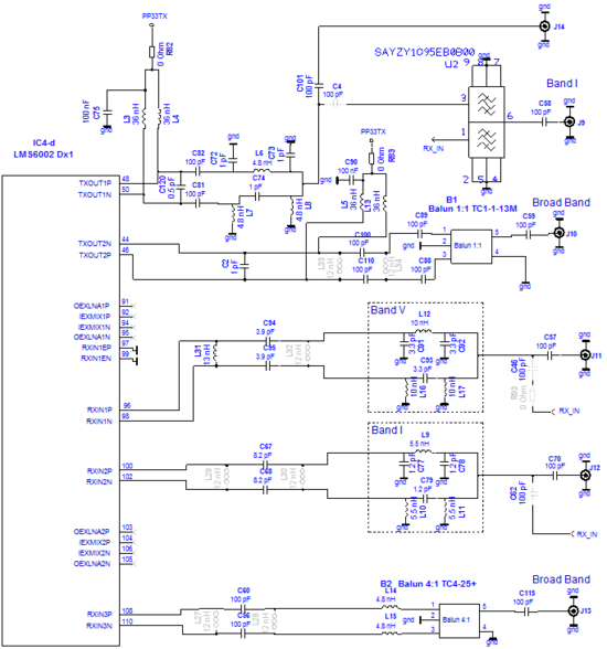
A typical application circuit of LMS6002D is given above. Note that only the RF part is shown. It is recommended all unused pins to be grounded, digital test pins should be left open while RF pins should be connected as indicated. As shown, RF ports are matched for UMTS bands I and V while TXOUT2 and RXIN3 are broadband matched. Refer to “LMS6002D Reference Design and PCB Layout Recommendations” for more details.
| |||||||||||||||||||||||||
