LimeADPD: Difference between revisions
AndrewBack (talk | contribs) m (AndrewBack moved page LimeMicro:Adaptive Digital Predistortion of RF Power Amplifiers to LimeADPD) |
AndrewBack (talk | contribs) No edit summary |
||
| Line 244: | Line 244: | ||
* Minor typographical and grammatical changes. | * Minor typographical and grammatical changes. | ||
{{ | {{Community}} | ||
Latest revision as of 10:23, 5 June 2017
Introduction
Power amplifiers (PA) are nonlinear devices and their linearisation is highly desired for a number of reasons. In case of radiofrequency (RF) PAs, linearisation improves power efficiency and subsequently reduces running cost of the wireless infrastructure.
Considering the PA performance for a given air interface, adjacent channel power ratio (ACPR) and error vector magnitude (EVM) are the key considerations to provide support for sophisticated modulation schemes, multicarrier signals, and high modulation bandwidths.
Here we present the Lime Microsystems solution for PA linearisation, based on adaptive digital predistortion (ADPD), for which the complete solution is Open Source and will be made available on GitHub and the LimeNET app store.
LimeADPD structure
Indirect learning architecture
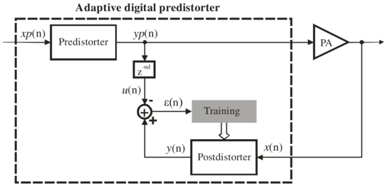
The simplified block diagram of an indirect learning architecture is given below. Please note that RF part in neither the TX (up to PA input) nor in RX (back to base band frequency) paths are shown for simplicity.
Delay line compensates ADPD loop ( to ) delay. Postdistorter is trained to be inverse of power amplifier. Predistorter is simple copy of postdistorter. When converged:
Hence, PA is linearised.
Complex valued memory polynomial
The LimeADPD algorithm is based on modelling nonlinear system (PA and its inverse, in this case) by complex valued memory polynomials. These are, in fact, cut versions of Volterra series, an approach well known for general nonlinear system modelling and identification. Here, "cut version" means the system can efficiently be implemented in real life applications.
For a given complex input:
complex valued memory polynomial produces complex output:
where:
are the polynomial coefficients while is the envelope of the input. For the envelope calculation two options are considered, the usual one:
and the squared one:
Typically, the squared option is used in ADPD applications since it is simpler to calculate and in most cases provides better results.
In the above equations, is memory length while represents nonlinearity order. Hence, complex valued memory polynomial can take into account both system memory effects and system nonlinearity.
LimeADPD equations
Based on discussions given in previous sections and using the signal notations of the above figure, the ADPD predistorter implements the following equations:
while the postdistorter does similar:
Note that predistorter and postdistorter share the same set of complex coefficients . The delay line is simple and its output is given by:
Training algorithm
The ADPD training algorithm alters complex valued memory polynomial coefficients in order to minimise the difference between PA input and PA output , ignoring the delay and gain difference between the two signals. Instantaneous error shown in the above figure is calculated as:
Training is based on minimising Recursive Least Square (RLS) error:
by solving a linear system of equations:
Any linear equation system solving algorithm can be used. LimeADPD involves LU decomposition, however iterative techniques such as Gauss-Seidel and Gradient Descent have been evaluated as well. LU decomposition is adopted in order to get faster adaptation and tracking of the ADPD loop.
Implementation platform
The ADPD algorithm is implemented using a LimeSDR-QPCIe board, a high level block diagram of which is shown below. The LimeSDR-QPCIe board has a lot more options than shown, including two LMS7002M chips, a USB interface, GPS receiver…) The LMS7002M itself is a 2T-2R RF IC. For clarity, the block diagram shows the minimum hardware options required to illustrate the LimeADPD implementation. Regarding the implementation, the same signal names as in the previous figure are used here.
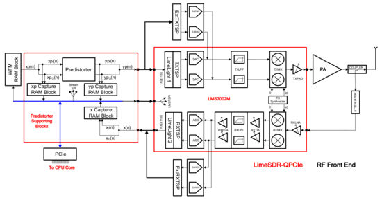
For development or demonstration, a test waveform is uploaded first and played from the WFM RAM Block. Initially, the predistorter is bypassed - i.e. , . The predistorter has provision for SPI in order to update the coefficients during the training. Signals , , and are captured using Data Capture RAM Blocks. Captured data is made available to the (Intel Motherboard) CPU Core via the PCIe interface. The CPU implements the postdistorter block, delay line, and the rest of training algorithm. After each adaptation step the CPU updates predistorter parameters via PCIe/Stream SPI.
In real applications WFM and Capture RAM blocks are not required. The algorithm needs only and as shown in LimeADPD structure. The CPU Core performs both ADPD adaptation, as explained above, and baseband (BB) digital modem functions which are application specific, for example Long Term Evolution (LTE).
As shown in the block diagram above, frequency conversion from BB to RF is performed by LMS7002M transmitter chains. Frequency down conversion from RF to BB is implemented by only one LMS7002M receive chain dedicated to ADPD; in other words, one receiver of the available RF RX chains is allocated as ADPD monitoring path. In case of MIMO applications, the same ADPD monitoring path is used as time sharing recourse to linearise multiple PAs which saves power consumption as well as on board RF resources.
Regarding data converters, the LimeSDR-QPCIe board offers two options: to use LMS7002M on-chip DACs/ADCs, or external ones. On-chip data converters are 12-bit devices, while external ones are 14-bit. 14-bit data converters are more suitable for ADPD if one wants to cancel IMD3 and IMD5 as well as to support wide band modulation schemes. If external data converters are used, the LMS7002M on-chip Transceiver Signal Processing blocks (TXTSP and RXTSP) are bypassed. In this case, minimum functionality required for ADPD to function is implemented by external counterparts shown as ExtTXTSP and ExtRXTSP in the block diagram above.
WFM and Data capture RAM Blocks are implemented using Altera Cyclone V FPGA resources and on-board RAM. More importantly, the same FPGA also implements predistorter, ExtTXTSP, ExtRXTSP blocks, PCIe, and other glue logic required to interconnect LimeSDR-QPCIe on board components including the two LMS7002M ICs to the CPU Core.
Measured Results
Before implementation and measurements, the ADPD algorithm has been thoroughly simulated. Simulation results are omitted from this document for clarity. ADPD performance has been measured and the results for two cases presented in this section.
Test Case 1:
- Moderate output power amplifier device Maxim Integrated MAX2612.
- Psat ~ 19dBm.
Test Case 2:
- MAX2612 is used as preamplifier stage followed by a Class-J GaN HEMPT amplifier.
- GaN amplifier drain efficiency ~ 70%.
- Psat ~ 40dBm.
Single carrier WCDMA Test Model 1 is used as test signal in both cases. ADPD memory and nonlinearity orders are set to , .
Test case 1: Maxim Integrated MAX2612 PA
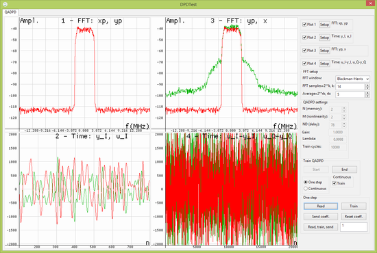
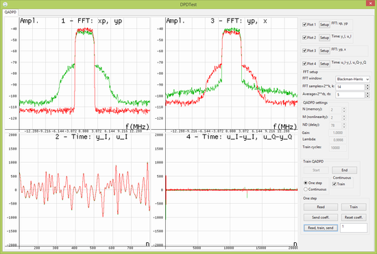
ADPD signals before training and ADPD signals after training show important ADPD signals before and after the algorithm convergence. Signals are captured by a graphical user interface (GUI) executed by the CPU Core.
Before training (ADPD signals before training), predistorter signals and are equal (plot 1). as a measure of PA output is distorted (plot 3). Waveforms and are very different (plot 2), resulting in huge error (plot 4) which ADPD has to minimise.
After ADPD training (ADPD signals after training), signal (plot 1) is predistorted in order to cancel PA distortion components. as a measure of PA output is now linearised (plot 3). There is an excellent match between and waveforms in both time and amplitude scale (plot 2). ADPD error (plot 4) is minimised. Improvement in PA linearisation can be seen by comparing the and spectra of plot 3.
ADPD signals before training
ADPD signals after training
RF PA output measurements are shown below.
PA output spectrum
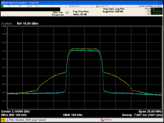
No ADPD – yellow trace. With ADPD – blue trace. IMD3 and IMD5 distortion components at the PA output reduced by almost 20 dB.
ACPR without ADPD
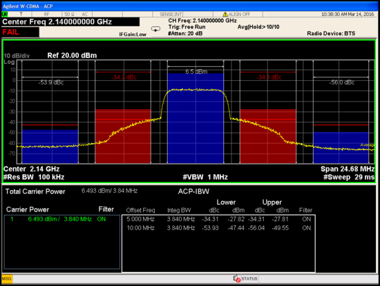
ACPR1 = -34 dBc, ACPR2 = -54 dBc.
ACPR with ADPD
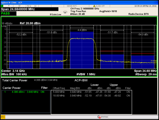
ACPR1 = -51 dBc, ACPR2 = -52 dBc.
EVM without ADPD
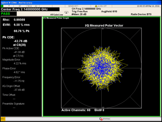
Measured at 6.58%.
EVM with ADPD
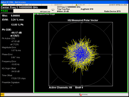
Measured at 3.24%.
Test case 2: Class-J GaN HEMPT amplifier
ACPR without ADPD
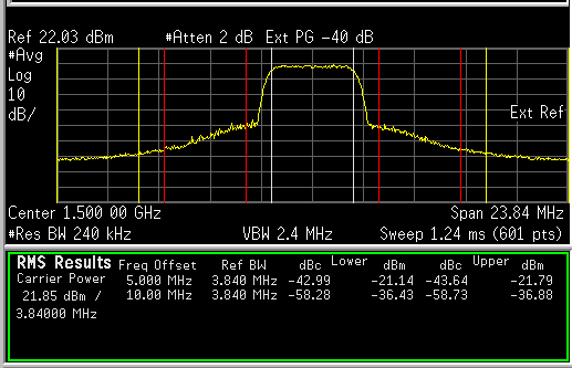
ACPR1 = -43 dBc, ACPR2 = -58dBc.
ACPR with ADPD
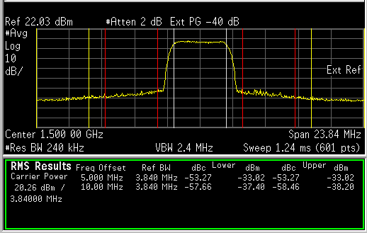
ACPR1 = -53 dBc, ACPR2 = -58dBc.
Conclusion
The LimeADPD algorithm has been confirmed by measured results. ADPD is capable of cancelling any distortion above system (DACs -> TX -> PA -> Coupler -> Attenuator -> RX -> ADCs) noise floor.
For test case 1, at antenna point (PA output) ACPR is improved from -34 dBc (out of spec.) to -51 dBc (well within the spec.) EVM is improved from 6.58% to 3.24%.
As far as linearisation is concerned, test case 2 is more challenging since there are two PA stages (MAX2612 followed by a Class-J GaN HEMPT amplifier) and both stages are nonlinear. Even in this case LimeADPD gives excellent results, i.e. ACPR is improved from -43 dBc (out of spec.) to -53 dBc (well within the spec.)
Work underway
- Test ADPD algorithm with 10W PAs covering different frequency bands.
- Check the performance with more demanding modulation schemes; using 5MHz, 10MHz, 15MHz, and 20MHz LTE as the test signal, for example.
- Modify the algorithm to linearise more than one PA for MIMO applications using single ADPD monitoring path.
- Test the algorithm performance in real applications, i.e. within the base station during voice, video, and data calls.
Document version
Based on Adaptive Digital Predistortion of RF Power Amplifiers Application Note v3r00.
Changes since document generation:
- Minor typographical and grammatical changes.
| |||||||||||||||||||||


