LimeSDR-USB User Guide: Difference between revisions
| Line 292: | Line 292: | ||
[[File:LimeSDR-USB-LMS7002-GUI-ConnectionSettings.jpg|center|550px|LMS7002 GUI showing ConnectingSettings option]] | [[File:LimeSDR-USB-LMS7002-GUI-ConnectionSettings.jpg|center|550px|LMS7002 GUI showing ConnectingSettings option]] | ||
Select "Cypress USB Streamer Example" for both the "LMS7 control" and "Stream board" , then click "Connect". | Select "Cypress USB Streamer Example" for both the "LMS7 control" and "Stream board" , then click "Connect". | ||
[[File:LimeSDR-USB-LMS7002-GUI-ConnectionSettings- | [[File:LimeSDR-USB-LMS7002-GUI-ConnectionSettings-3.png|center|550px|LMS7002 GUI showing Connection Settings window]] | ||
===Uploading the bitstream to the FPGA=== | ===Uploading the bitstream to the FPGA=== | ||
Latest revision as of 12:56, 29 August 2017
About
The LimeSDR-USB development board provides a hardware platform for developing and prototyping high-performance and logic-intensive digital and RF designs using Altera’s Cyclone IV FPGA and Lime Microsystems LMS7002M transceiver.
For more information on the following topics, refer to the respective documents: Cyclone IV Device Handbook LMS7002M transceiver resources
Key features
USB interface
- Cypress FX3 Super Speed USB 3rd generation controller
FPGA features
- Cyclone IV EP4CE40F23C8N device in 484-pin FPGA
- 39,600 logic elements
- 1,134Kbits embedded memory
- 116 embedded 18x18 multipliers
- 4 PLLs
FPGA configuration
- JTAG mode configuration
- Active serial mode configuration
- Possibility to update FPGA gateware by using FX3 (USB)
Memory devices
- 2x 1Gbit (64M x 16) DDR2 SDRAM
- 4Mbit flash for FX3 firmware
- 16Mbit flash for FPGA gateware
- 3x 64K (8K x 8) EEPROMs for LMS MCU firmware, LMS MCU data, and FX3 data
Connections
- 6-12V DC power jack
- FPGA GPIO headers
- Micro-USB 3.0 (Type B) connector or USB 3.0 (Type A) plug
- Coaxial RF (U.FL) connectors
Clock system
- 30.72MHz ±250 ppb on-board VCTCXO
- Possibility to lock VCTCXO to external clock or tune VCTCXO by onboard DAC
- Programmable clock generator for the FPGA reference clock input or LMS PLLs
Board size
- Board Size 60mm x 100mm (2.36” x 3.94”)
Board overview
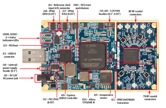
LimeSDR-USB board version 1.2 with highlighted major connections. There are three connector types: data and debugging (USB 3.0, FPGA GPIO, and JTAG), power (DC jack and external supply pin header), and high frequency (RF and reference clock).
Board components
Featured devices
| Board reference | Type | Description |
|---|---|---|
| IC1 | FPRF | Field programmable RF transceiver, LMS7002M |
| IC31 | FPGA | Altera Cyclone IV, EP4CE40F23C8N 484-BGA |
| IC6 | USB 3.0 microcontroller | Cypress FX3 Super Speed USB 3rd generation controller, CYUSB3014 |
Miscellaneous devices on board
| Board reference | Type | Description |
|---|---|---|
| IC32 | IC | Quad SPDT switch, TS3A5018PW |
| IC9 | IC | Temperature sensor, LM75 |
| IC12 | IC | SPI to I²C bridge, SC18IS602BIPW |
| IC10 | IC | I²C port expander with 4 push-pull outputs and 4 inputs, MAX7322ATE+ |
Configuration, status, and setup elements
| Board reference | Type | Description |
|---|---|---|
| R168, R169, R170, R171, R174, R175, R178, R179 | 0 Ohm resistor | FPGA (IC31) MSEL[3:0]. Active Serial Standard configuration scheme is selected by default. |
| R75, R76, R77, R79 | 10 kOhm resistor | USB3.0 microcontroller (IC6) boot configuration resistors |
| J12 | JTAG chain pin header | USB 3.0 microcontroller's (IC6) debugging pin header, 0.05" pitch |
| J13 | Pin header | USB 3.0 microcontroller (IC6) boot source (flash or USB), 0.05" pitch |
| SW1 | Push-button | USB 3.0 microcontroller (IC6) reset button |
| J17 | JTAG chain pin header | FPGA (IC31) programming pin header for Altera USB-Blaster download cable, 0.05" pitch |
| LEDS1 | Red-green status LEDs | User defined FPGA (IC31) indication LED1 (nearest board edge if SMD, on the bottom if through-hole); user defined FPGA indication LED2 (farthest board edge if SMD, on the top if through-hole) |
| LEDS2 | Red-green status LEDs | USB 3.0 microcontroller (IC6) status indication LED (nearest board edge if SMD, on the bottom if through-hole); board power indication LED (farthest board edge if SMD, on the top if through-hole) |
General user input/output
| Board reference | Type | Description |
|---|---|---|
| J18 | Pin header | 8 FPGA GPIOs, 0.1" pitch |
| J19, J20 | Pin header | 3.3V fan connection pin headers, 0.1" pitch (J19) and 0.05" pitch (J20) |
Memory devices
| Board reference | Type | Description |
|---|---|---|
| IC4, IC5 | DDR2 memory | 1Gbit (64M x 16) DDR2 SDRAM with a 16-bit data bus |
| IC2, IC3 | EEPROM | 64K (8K x 8) EEPROM, LMS7002 (IC1) MCU firmware (IC2), LMS7002M (IC1) data (IC3) |
| IC11 | EEPROM | 64K (8K x 8) EEPROM, USB 3.0 microcontroller (IC6) EEPROM |
| IC33 | Flash memory | 16Mbit flash for FPGA (IC31) configuration |
| IC8 | Flash memory | 4Mbit flash for USB 3.0 microcontroller (IC6) firmware |
Communication ports
| Board reference | Type | Description |
|---|---|---|
| J11 | USB 3.0 connector | Micro-USB 3.0 (Type B) connector or USB 3.0 (Type A) plug |
Clock circuitry
| Board reference | Type | Description |
|---|---|---|
| XT4 | VCTCXO | 30.72MHz oscillator, E5280LF |
| IC17 | IC | Programmable clock generator for the FPGA (IC31) reference clock input and RF boards |
| IC16 | IC | Clock synthesiser, ADF4002 |
| J14 | U.FL connector | RF connector for external clock |
| IC15 | IC | DAC for TCXO (XT4) frequency tuning |
Power supply
| Board reference | Type | Description |
|---|---|---|
| J15 | DC input jack | External 6V - 12V DC power supply |
| J16 | Pin header | External 6V - 12V DC power supply |
Board components, top side
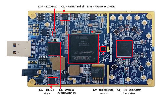
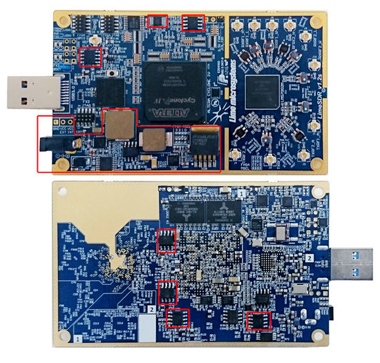
LimeSDR-USB board version 1.2 pictured with highlighted components on the top side.
Board components, bottom side
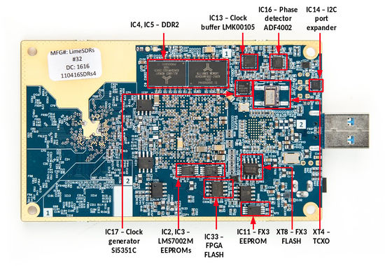
LimeSDR-USB board version 1.2 pictured with highlighted components on the bottom side.
LimeSDR-USB board architecture
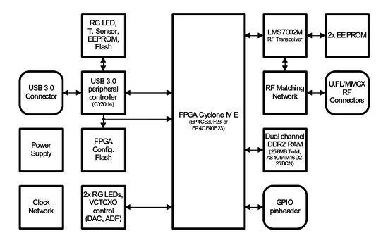
The heart of the LimeSDR-USB board is an Altera Cyclone IV FPGA. It’s main function is to transfer digital data between the PC and the radio through a USB 3.0 connector.
LMS7002M-based connectivity
Digital interface signals
LMS7002 is using data bus LMS_DIQ1_D[11:0] and LMS_DIQ2_D[11:0], LMS_ENABLE_IQSEL1 and LMS_ENABLE_IQSEL2, LMS_FCLK1 and LMS_FCLK2, LMS_MCLK1 and LMS_MCLK2 signals to transfer data to/from FPGA. Indexes 1 and 2 indicate transceiver digital data PORT-1 or PORT-2. Any of these ports can be used to transmit or receive data. By default PORT-1 is selected as transmit port and PORT-2 is selected as receiver port. The FCLK# is input clock and MCLK# is output clock for LMS7002M transceiver. TXNRX signals sets ports directions. For LMS7002M interface timing details refer to LMS7002M transceiver datasheet pages 12-13.
SPI interface
LMS7002M transceiver is configured via 4-wire SPI interface: FPGA_SPI0_SCLK, FPGA_SPI0_MOSI, FPGA_SPI0_MISO, FPGA_SPI0_LMS_SS. The SPI interface is controlled from FPGA Bank 8 (VDIO_LMS_FPGA, 3.3V).
I²C interface
The I²C interface is used to control external clock synthesiser on UNITE7002 board. The signals LMS_I2C_CLK and LMS_I2C_DATA are connected to FPGA Bank 8 (VDIO_LMS_FPGA, 3.3V).
Control signals
These signals are used for optional functionality.
- LMS_RXEN, LMS_TXEN – receiver and transmitter enable/disable signals connected to FPGA Bank 8 (VDIO_LMS_FPGA, 3.3V).
- LMS_RESET – LMS7002M reset connected to FPGA Bank 7 (VDIO_LMS_FPGA, 3.3V).
SDRAM
The LimeSDR-USB board has two 128 MB (16-bit bus) DDR2 SDRAM ICs (AS4C64M16D2-25BCN) connected to double data rate pins onCyclone IV 1.8V Bank 2, Bank 3 and Bank 4. RAM chips are connected to separate memory controllers to operate in dual channel mode. The memory can be used for data manipulation between transceiver and FPGA at high date rates.
USB 3.0 controller
Software controls the LimeSDR-USB board via the USB 3.0 microcontroller (CYUSB3014). The data transfer to/from the board, SPI communication, and FPGA configuration are all done via the USB 3.0 controller.
- FX3_DQ[31:0] – FX3 32-bit GPIF data interface is connected to Cyclone IV 1.8V Bank 5.
- FX3_CTL[8:0], [12:11] – FX3 GPIF interface control signals.
- FX3_PCLK – GPIF interface clock
- GPIO[26:25] – FX3 (USB) status LED (LED5).
- FX3 SPI interface – program IC8 flash memory, boot from IC8 flash memory.
- FX3 I²C bus – connected to the I2C to SPI bridge IC12, I2C port expander IC10, temperature sensor IC9 and EEPROM memory IC11.
- PMODE[2:0] – boot options, by default boot from SPI and USB boot is enabled. If J13 jumper is present FX3 will boot from IC8 flash memory if correct firmware exists.
- SW1 – resets FX3
- J12 – FX3 JTAG programming/debugging pin header.
Indication LEDs
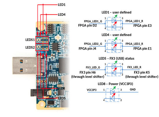
The LimeSDR-USB board comes with four indication LEDs: LEDS1 (LED1, LED4) and LEDS2 (LED5, LED8). LED1, LED4 and LED5 are user defined and connected to the FPGA and USB 3.0 controller as shown. LED8 is hardwired to VCC3P3 power rail and is lit up whenever the board is powered on. By default, dual-colour SMD LEDs are populated and through-hole LEDs are unpopulated. If required, the user can fit dual-colour 3mm diameter through-hole LEDs with a dedicated right-angle plastic holder.
Low-speed interfaces
The LimeSDR-USB board's low speed interfaces are divided into FX3 and FPGA groups. The following block diagrams depict the main ICs, corresponding IC pin numbers, data buses, and serial protocol addresses.
FX3 low-speed interfaces
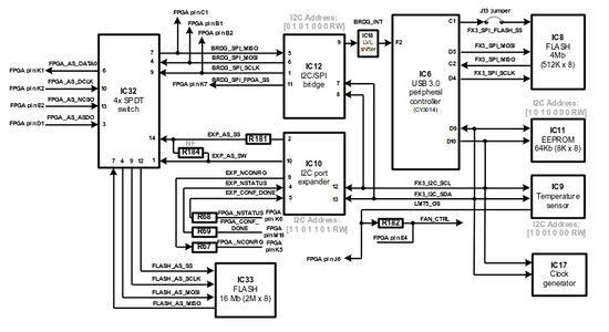
LimeSDR-USB board peripherals are controlled via the USB interface. All commands that comes from USB are firstly processed by the FX3 controller. If an I²C peripheral (temperature sensor, port expander, clock generator) on FX3_I2C bus must be controlled this can be done directly. FX3_I2C is also connected to the FPGA.
FPGA low-speed interfaces
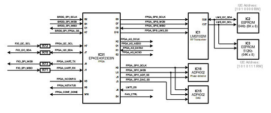
FX3 hardware SPI cannot be used if the 32-bit GPIF interface is configured. If SPI (RFIC, frequency synthesiser, clock generator) devices must be controlled by FX3, firstly it transfers data to I²C-SPI bridge. Depending on required SPI slave device, there could several possibilities:
- Flash for FPGA gateware: using SPDT switch (IC32) flash memory is switched from FPGA to I²C-SPI bridge. Then flash content is updated and flash memory is switched back to FPGA. This is done to update the FPGA gateware in flash memory.
- FPGA: FPGA has its own SPI module and can be controlled as regular SPI device. By using FPGA SPI it is possible to control FPGA modes, etc. The FPGA can also act as bridge between BRDG_SPI and FPGA_SPI0 or FPGA_SPI1.
- RFIC, clock synthesiser, clock generator: to control a device on FPGA_SPI0 or FPGA_SPI1 from BRDG_SPI, the FPGA must be configured to select the corresponding slave device and then it operates as bridge. When the transaction with the slave is completed, the slave must be deselected.
If FX3 firmware flash memory content must be updated, then FX3 switches to 16-bit GPIF mode to directly accesses flash content.
Clock distribution
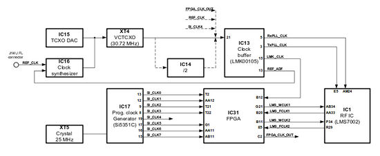
The LimeSDR-USB board has an on-board 30.72 MHz ±250 ppb VCTCXO that acts as a reference clock for LMS_PLLs. The on-board frequency synthesiser (ADF4002) is used to synchronise the on-board VCTCXO with external equipment (via the J14 U.FL connector) to calibrate frequency error. On-board DAC also can be used to tune VCTCXO. At the same time only ADF or DAC can control VCTCXO. DAC and ADF is controlled by FX3 (SUB) and selection between ADF and DAC is done automatically. The J14 connector can also be used to supply external reference clock (by fitting R106 and removing R96, C212). The programmable clock generator (Si5351C) can generate any reference clock frequency, starting from 8 kHz – 160 MHz, for FPGA and LMS PLLs
Power distribution
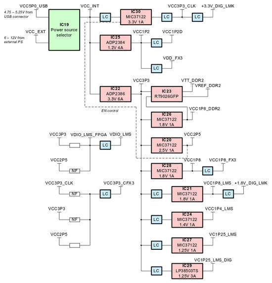
The LimeSDR-USB board can be powered from its USB port. In applications where USB power is insufficient, the board can be powered from an external 6 – 12 V power supply. External power can be fed to the J18 barrel power connector using power plug (1.35mm ID, 3.5mm OD) or pin header J19 (GND and VCC_EXT). The LimeSDR-USB board has automatic source selection between USB and external source, with polarity protection.
Driver installation
The communication between the LimeSDR-USB board and a host PC running the lms7suite software is done via the USB 3.0 interface. The LimeSDR-USB board comes with pre-programmed FX3 firmware and is ready to use. If the FX3 firmware needs to be updated, follow the instructions in Flashing the USB 3.0 microcontroller.
Windows driver installation
THIS DOCUMENT HAS NOT BEEN UPDATED IN SOME TIME AND THIS SECTION SHOULD BE IGNORED
For Windows O/S driver installation follow the Lime Suite documentation instead.
Download the latest Cypress EZ-USB FX3 Software Development Kit drivers, select the cy_ssusbsuite_vn.n.n.zip package (where n.n.n represents the version number), and extract its contents. Connect the LimeSDR-USB board to a USB 3.0 port on the host PC, then perform the following steps:
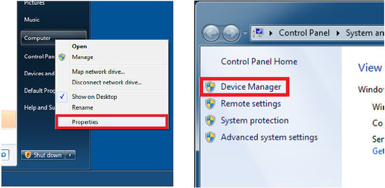
- Click "Start", right click on "Computer", click "Properties" then click "Device Manager."
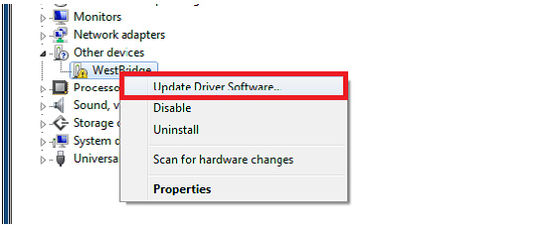
- With the LimeSDR-USB board connected to the host PC, click on "Other devices," expand it, right-click on "WestBridge," then click "Update Driver Software" from the pop-out menu.
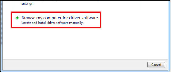
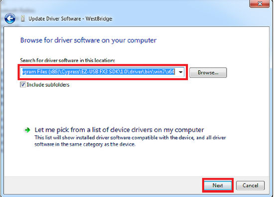
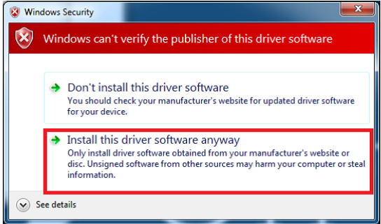
- Click "Browse my computer for driver software" and choose the driver from downloaded package suitable for your version of Windows and CPU type. Click "Next," then click "Install this driver software anyway" when prompted to confirm installation of an unsigned driver.
- Windows version:
- Windows XP: wxp
- Windows Vista: vista
- Windows 7: win7
- Windows 8: win8
- Windows 8.1: win81
- CPU type:
- x86: 32bit-i386
- x64: 64bit-amd64
- Windows version:
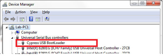
- Following the installation of the driver, a "Cypress USB BootLoader" device will appear in "Device Manager" under "Universal Serial Bus controllers". Installation is now complete and the LimeSDR-USB ready to use.
NOTE: If you are using a 64-bit version of Windows 7, you must disable driver signature enforcement. To do this, restart the host PC, press F8 at startup, and choose "Disable Driver Signature Enforcement." This need only be carried out once. NOTE: If you are using Windows 8 or later, follow these instructions to disable driver signature enforcement.
Linux driver installation
The USB 3.0 drivers for the LimeSDR-USB are included in the libusb library, which is installed by default in most Linux distributions. Manual installation of specific drivers is not required.
Flashing the USB 3.0 microcontroller
THIS DOCUMENT HAS NOT BEEN UPDATED IN SOME TIME AND THIS SECTION SHOULD BE IGNORED
For updating the FX3 firmware please follow the Lime Suite documentation instead.
To install updated or custom firmware on the FX3 USB 3.0 microcontroller, first download and extract the "CyControl.exe" application from the cy_ssusbsuite_vn.n.n.zip package. Cypress FX3 USB microcontroller has an integrated boot loader, which starts automatically after power-up or reset. If the flash memory is empty or connector J17 on the LimeSDR-USB is open, the USB 3.0 microcontroller boots with the factory default firmware. Run the "USB Control Center" application on the host PC and in the menu click "Cypress USB BootLoader".
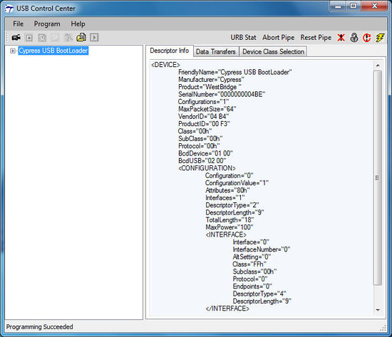
There are two ways of uploading the firmware to USB3 microcontroller:
- Program the internal RAM memory, as described in Uploading firmware to the FX3 RAM. The memory will be cleared after first power cycle, restoring the previous firmware.
- Program the external flash memory connected to the USB 3.0 controller, as described in Uploading firmware to empty flash and Uploading firmware to non-empty flash. The USB 3.0 microcontroller will boot from the new firmware you have installed to its flash memory after every power on.
Uploading firmware to the FX3 RAM
Start the "CyControl.exe" application and click "Cypress USB BootLoader". Click the menu command "Program FX3 RAM". In the new pop-up window, select your new firmware image file (file extension "*.img") and click "Open". The status bar of the USB Control Center application will indicate "Programming RAM". This message will change to "Programming succeeded" after programming is complete. If you expand the "Cypress USB StreamerExample" entry in USB Control Center application now, you will see the new USB configuration.
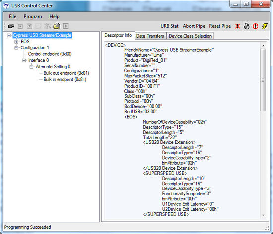
Uploading firmware to empty flash
If the external flash connected to the FX3 USB 3.0 microcontroller is empty, short jumper J17 then connect the LimeSDR-USB board to the host PC. Start the "CyControl.exe" application and click "Cypress USB BootLoader" Click the menu command "Program FX3 SPI FLASH". The status bar of the USB Control Cneter application will indicate "Waiting for Cypress Boot Programmer device to enumerate", then after some time a pop-up window will appear. Select your new firmware image file (file extension "*.img") and press "Open". The status bar will indicate "Programming of SPI FLASH in Progress". This message will change to "Programming succeeded" after flash programming is complete. NOTE: The USB 3.0 microcontroller will boot from firmware uploaded to flash at every power-on if jumper J3 is shorted.
Uploading firmware to non-empty flash
To update the FX3 USB 3.0 microcontroller's flash memory with new firmware, follow these steps:
- Disconnect the LimeSDR-USB from the host PC's USB port.
- Make sure that jumper J17 is open.
- Connect the LimeSDR-USB board to the host PC's USB port.
- Short jumper J17.
- Follow the procedure listed in Uploading firmware to empty flash.
Loading a custom bitstream to FPGA
Connecting to the board
To load a bitstream file to the LimeSDR-USB's FPGA, launch the "lms7suite" application and click "Options", then "ConnectionSettings".
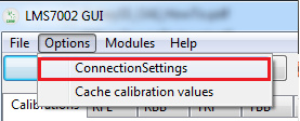
Select "Cypress USB Streamer Example" for both the "LMS7 control" and "Stream board" , then click "Connect".
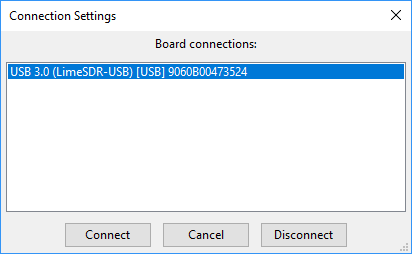
Uploading the bitstream to the FPGA
The Altera Cyclone IV FPGA which sits on the LimeSDR-USB board can be programmed using the "lms7suite" software. To program the bitstream into the FPGA, click "Modules" then click "Programming" from the drop down menu.
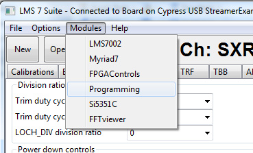
A new control section will appear in the bottom of the main window.

This section allows the loading of raw binary files (*.rbf) to the FPGA, with three programming modes.
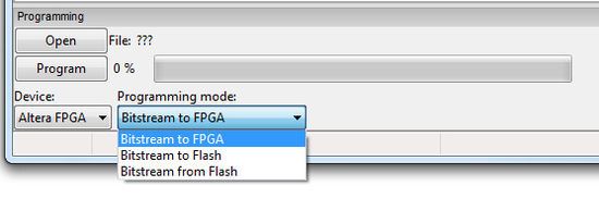
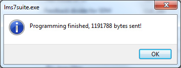
Choose the "Bitstream to Flash" programming mode. This loads a raw binary file from the host PC to the FPGA's external flash memory. Select your bitstream file by clicking "Open" and initiate flash memory programming by clicking "Program." A confirmation dialogue will appear when programming is completed.
Document Version
Based on LimeSDR-USB v1.2 User Manual, Version 00.06.
Changes since document generation:
- Minor typographical and grammatical changes.
- Extended instructions in Windows driver installation.
| |||||||||||||||||||||
