ClockTamerFeaturesAndTechnicalSpecification
Output types
ClockTamer comes with one or more of the following output types:
- CMOS. Single-ended output, <3V peak-to-peak. The most popular option for low output frequencies (<200 MHz)
- LVDS. Differential output, <0.5V peak-to-peak. Useful if you want to generate frequencies above 200 MHz. Requires correct termination of both ends of LVDS output; you cannot use one end and leave the other floating!
- half-LVDS. Single-ended output, <0.5V peak-to-peak. In half-LVDS outputs only positive end (N+) is accessible to a user, while negative end (N-) is terminated with 50 Ohm resistor on the ClockTamer PCB. This output has the same frequency limitation as CMOS (<200 MHz), but has lower peak-to-peak voltage.
USRP users can use either CMOS or half-LVDS outputs, although CMOS is the default and most popular option.
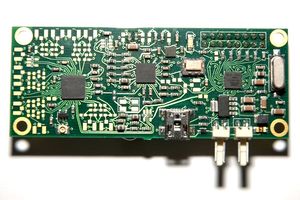
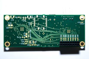
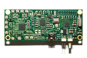
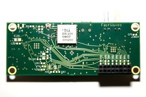
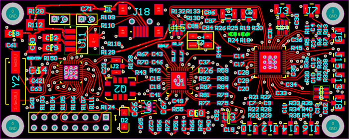
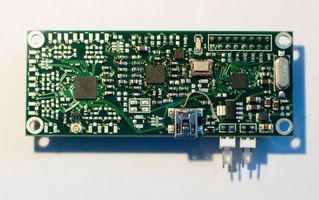
ClockTamer-1.2
ClockTamer-1.2 with a single CMOS output and no GPS:
ClockTamer-1.2 with all outputs and GPS:
Specifications
| Output clock temperature stability | 0.28ppm in 0-70C temperature range (without GPS option) or 50ppb with GPS option |
| Outputs | up to 2 CMOS outputs up to 5 LVDS outputs (default is 1 CMOS and 0 LVDS outputs) |
| Output connector type | U.FL |
| Input power voltage | 3.7 - 6.0V |
| Input power types | miniUSB (enough to power !ClockTamer with 1 or 2 outputs with or without GPS) or 6V 2-pin connector (it has 2 connectors to connect into daisy-chain with USRP fan) |
| Surge protection | 6V power input is protected with fast acting resetable fuse |
| Size | 35mm x 86mm x 14mm |
| Control | miniUSB and SPI (16-pin connector for easy connection to USRP) |
Output frequencies
The output frequency can be set with 1Hz precision (this is a firmware limitation and could be fixed in later firmware versions). Tuning is possible within the following ranges:
|   | CMOS | LVDS/LVPECL |
| 3.75 - 94.75 MHz | X | X |
| 95.20 - 113.70 MHz | X | X |
| 119.00 - 142.13 MHz | X | X |
| 158.67 - 189.50 MHz | X | X |
| 238.00 - 284.25 MHz | X | |
| 476.00 - 568.50 MHz | X | |
| 952.00 - 1137.00 MHz | X |
Schematics, PCB layout and bill of materials
Schematics
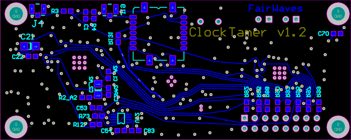
PCB layout (click for larger version)
Bill of materials
Datasheets of the most important parts:
- Atmel ATMega (AT90USB162/AT90USB82) - (PDF)
- Connor Winfield D75A (TCXO, 10MHz/20MHz 0.28ppm) - (PDF)
- National Semiconductor LMX2531LQ1515E/LMX2531LQ2080E (PLL + fractional VCO) - (PDF)
- National Semiconductor LMK01000/LMK01010 (Clock Buffer, Divider, and Distributor) - (PDF)
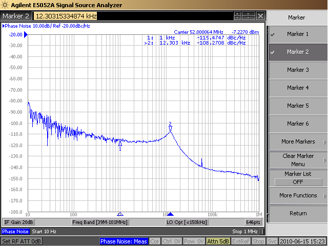
Phase noise
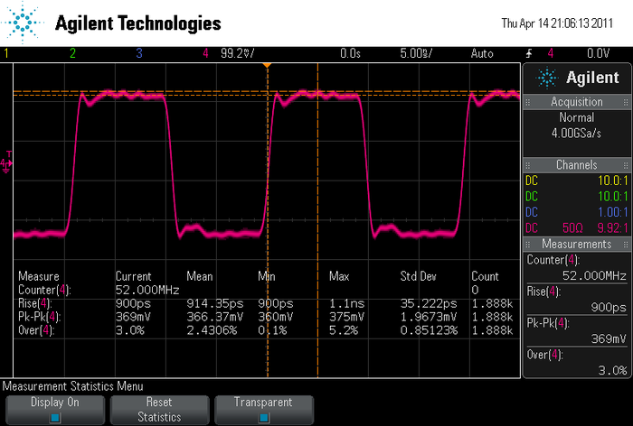
Measured for 52MHz output.
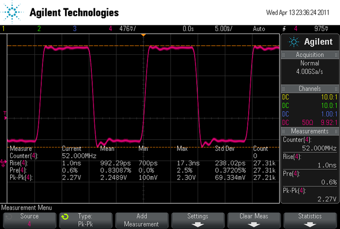
Output waveform
Measurements made by Sylvain Munaut.
USRP is modified with 51R resistor across the SMA socket on the USRP.

Measured with a 350 MHz scope and a 4GHz active probe freshly calibrated with as short a ground lead as you can make.

It shows a dead center 2 Vpp, low ringing, and fast enough rise time to meet the USRP clock chip input requirements.
'Measurement for ClockTamer CMOS output
Measurement for ClockTamer single-ended LVDS output
ClockTamer-1.1
Specifications
| Output clock temperature stability | 0.28ppm in 0-70C temperature range (without GPS option) or 50ppb with GPS sync option |
| Outputs | up to 2 CMOS outputs up to 3 LVPECL/LVCMOS outputs up to 2 LVDS outputs (default is 1 CMOS, 0 LVPECL/LVCMOS and 0 LVDS outputs) |
| Output connector type | U.FL |
| Power | miniUSB or 6V 2-pin connector (2 inputs to connect into daisy-chain with USRP fan) |
| Surge protection | 6V power input is protected with fast acting resetable fuse |
| Size | 35mm x 86mm x 14mm |
| Control | miniUSB and SPI (16-pin connector for easy connection to USRP) |
Output frequencies
Output frequency can be set with 1Hz precision (this is a firmware limitation and could be fixed in later firmware versions). Tuning can be done in the following ranges:
| CMOS | LVDS/LVPECL | |
| 1.42 - 32.92 MHz | X | X |
| 32.95 - 35.91 MHz | X | X |
| 36.25 - 39.50 MHz | X | X |
| 40.28 - 43.89 MHz | X | X |
| 45.31 - 49.38 MHz | X | X |
| 51.79 - 56.43 MHz | X | X |
| 60.42 - 65.83 MHz | X | X |
| 72.50 - 79.00 MHz | X | X |
| 90.63 - 98.75 MHz | X | X |
| 120.83 - 131.67 MHz | X | X |
Schematics, PCB layout and bill of materials
Bill of materials
Schematics
These are the same as ClockTamer-1.2.
PCB layout
PCB layout has only minor changes compared ClockTamer-1.2
