Lime-GPSDO v1.0 hardware description
Lime-GPSDO Board Key Features
The Lime-GPSDO development board provides high stability clock source for timing sensitive applications. Clock frequency is being constantly monitored inside MAX10 FPGA and tuned by PPS signal from GNSS module.

For more information on the following topics, refer to the respective documents:
Lime-GPSDO board features:
- USB Interface
- Silicon labs USBXpress Family USB-to-UART bridge CP2102N.
- FPGA Features
- MAX10 10M16SAU169C8 device in 169-pin UBGA
- 16K logic elements
- 549 Kbits embedded memory (M9K) and 2368 Kbits of user Flash Memory
- 45 embedded 18x18 multipliers
- 1 PLLs
- FPGA Configuration
- JTAG mode configuration
- Memory Devices
- 4Mbit FLASH
- 128Kbit (16K x 8) EEPROM
- Connections
- microUSB2.0 (type B)
- SMA connectors for clock IN/OUT, time pulse output and GNSS antenna
- FPGA GPIO header (0.05” pitch)
- FPGA JTAG connectors (0.05” pitch and side connector)
- 5V DC power jack and pinheader
- Backup battery connector for GNSS receiver
- Clock output pinheader
- External UART connector
- External I2C connector
- Clock System
- 30.72MHz VCOCXO:
- Frequency calibration ±0.5ppm;
- Frequency stability over temperature in still air ±20ppb;
- Frequency slope ΔF/ΔT in still air ±1.2ppb/°C
- Possibility to tune VCOCXO by onboard DAC
- Possibility to use GNSS PPS signal as a reference when tuning VCOCXO frequency
- 30.72MHz VCOCXO:
- Board Size without connectors 50.50mm x 80mm (1.99” x 3.15”)
Board Overview
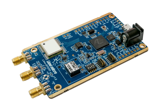
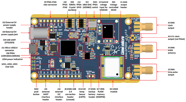
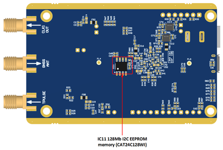
Lime-GPSDO board version 1.0 picture with highlighted major components and connections presented in Figure 1 and Figure 2. There are three connector types – data and debugging (USB2.0, FPGA GPIO and JTAG), power (DC jack and external supply pinheader), clock source output, GNSS antenna and time pulse output.


Board components description listed in the Table 1 and Table 2.