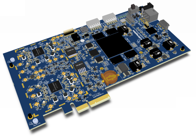
LimeSDR-QPCIe v1.2 hardware description
Introduction
LimeSDR-QPCIe is low-cost software defined radio board based on Lime LMS7002M Field Programmable Radio Frequency (FPRF) transceiver and Altera Cyclone V PFGA, through which apps can be programmed to support any type of wireless standard, e.g. UMTS, LTE, LoRa, GPS, WiFi, Zigbee, RFID, Digital Broadcastimng, Radar and many more.

For more information on the following topics, refer to the respective documents:
- Cyclone V device family, refer to Cyclone V Device support resources link
- LMS7002M transceiver resources link
LimeSDR-QPCIe v1.2 board features:
- USB Interface
- Cypress FX3 Super Speed USB 3rd generation controller
- FPGA Features
- Cyclone V, 5CGXFC7D7F31C8N device in 896-pin FBGA package
- 150’000 logic elements
- 6860 Kbits embedded memory
- 312 embedded 18x18 multipliers
- 7 PLLs
- 9 Transceivers (2.5Gbps)
- PCIe Hard IP Blocks
- 2 Hard Memory Controllers
- FPGA Configuration
- JTAG mode configuration
- Active serial mode configuration
- Possibility to update FPGA gateware by using FX3 (USB)
- Possibility to update FPGA gateware by using PCIe interface.
- RF
- 2x LMS7002M, FPRF transceivers
- Onboard RSSI measurement circuits
- Onboard loopback control switches
- DACs and ADCs
- 2x DAC5672A, dual, 14-bit, Digital-To-Analog converters
- 1x ADS424, Dual-Channel, 14-bit, Analog-To-Digital converter
- Memory Devices
- 4 x 2Gbit DDR3 SDRAM (128M x 16)
- 4Mbit flash for FX3 firmware
- 128Mbit flash for FPGA gateware
- 2 x 128Kbit and 2 x 512Kbit EEPROMs for LMS MCU firmware, LMS MCU data
- 1 x 128K EEPROM for FX3 or FPGA data
- Connections
- microUSB3.0 (type B) connector
- PCIe x4 edge connector (Gen1)
- Coaxial RF (U.FL) connectors
- 2x PMOD header (0.1” pitch)
- FPGA (0.1” pitch) and FX3 (0.05” pitch) JTAG connectors
- 12V DC power jack and pinheader
- LVDS connector (0.05” pitch)
- Fan connector (12V/5V)
- PCIe 6-pin power connector
- Holder for coin cell CR1220 battery
- Clock System
- 30.72MHz VCTCXO (precision: ±1 ppm initial, ±4 ppm stable).
- Possibility to lock VCTCXO to external clock using ADF4002 or tune VCTCXO by onboard DAC (AD5662)
- Programmable clock generator for the FPGA reference clock input or LMS PLLs
- VCTCXO clock output for external device synchronization.
- 1x 100 MHz, 4 x 125MHz crystal oscillators for FPGA
- Miscellaneous devices
- LM75 Digital temperature sensor with 2-Wire Interface.
- DS3231 real-time clock.
- M0578-A3 GPS/GNSS module receiver
- Board Size 190mm x 106.7mm (7.48” x 4.20”)
LimeSDR-QPCIe Board Overview
LimeSDR-QPCIe board version 1.2 picture with highlighted major connectors presented in Figure 2. There are three connector types – data and debugging (PCIe, USB3.0, PMOD, LVDS and JTAG), power (DC jack and external supply pinheaders) and high frequency (RF and reference clock).
///////////// Figure 2 LimeSDR-QPCIe v1.2 Development Board Connectors
Board components description listed in the Table 1 and Table 2.