LimeSDR-PCIe v1.2 hardware description
Draft
Introduction
LimeSDR-PCIe is low-cost software defined radio board based on Lime LMS7002M Field Programmable Radio Frequency (FPRF) transceiver and Altera Cyclone IV GX PFGA, through which apps can be programmed to support any type of wireless standard, e.g. UMTS, LTE, LoRa, GPS, WiFi, Zigbee, RFID, Digital Broadcasting, Radar and many more.
Complete Development Kit Package
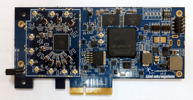
The LimeSDR-PCIe v1.2 board from full package showed in Figure 1.

Development kit content:
- LimeSDR-PCIe v1.2 board
- USB stick containing following files:
- Doc/ - Documentation files for LimeSDR-PCIe
- Drivers/ - Windows drivers for LimeSDR-PCIe
- Gateware/ - FPGA gateware related files for LimeSDR-PCIe v1.2
- Gui/ - LimeSuiteGUI software and related files
LimeSDR-PCIe Board Key Features
The LimeSDR-PCIe development board provides a hardware platform for developing and prototyping high-performance and logic-intensive digital and RF designs using Altera’s Cyclone IV GX FPGA and Lime Microsystems transceiver.
LimeSDR-PCIe board features:
- RF transceiver:
- Lime Microsystems LMS7002M
- FPGA Features
- Cyclone IV GX (EP4CGX30CF23C7N) device in 484-pin FBGA
- 29’440 logic elements
- 1080 Kbits embedded memory
- 80 embedded 18x18 multipliers
- 4 general and 2 multipurpose PLLs
- 4 high-speed transceivers
- PCIe (PIPE) hard IP block
- FPGA Configuration
- JTAG mode configuration
- Active serial mode configuration
- Possibility to update FPGA gateware by using PCIe interface
- Memory Devices
- 2x 1Gbit (64M x 16) dual channel DDR2 SDRAM
- 4Mbit flash for FPGA data
- 64Mbit flash for FPGA gateware
- 128Kb (16K x 8) EEPROM for LMS MCU firmware and 512Kb (64K x 8) LMS MCU data
- Connections
- PCI Express x4 (4 lanes)
- Coaxial RF (U.FL) connectors
- FPGA GPIO 2x8 (3.3V) headers
- FPGA and JTAG connector
- DC (12V) power jack and pinheader
- FAN (12V) connector
- Clock System
- 30.72MHz ±250 ppb onboard VCTCXO
- Possibility to lock VCTCXO to external clock or tune VCTCXO by onboard DAC
- Programmable clock generator for the FPGA reference clock input or LMS PLLs
- 100 MHz and 2x 50MHz crystal oscillators for FPGA
- Board Size 68,9mm x 136,85mm
For more information on the following topics, refer to the respective documents:
- Cyclone IV device family, refer to Cyclone IV Device Handbook [link]
- LMS7002M transceiver resources [link
LimeSDR-PCIe board overview
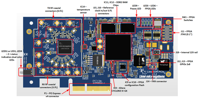
LimeSDR-PCIe board version 1.2 picture with highlighted major connections and components presented in Figure 1 and Figure 2. There are three connector types – data and debugging (PCIe, FPGA GPIO and JTAG), power (DC jack - optional) and high frequency (RF and reference clock). LimeSDR-PCIe board version 1.2 picture with highlighted components on top presented in Figure 1.

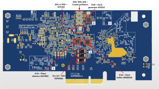
LimeSDR-PCIe board version 1.2 picture with highlighted components on bottom presented in Figure 2

Board components description listed in the Table 1.
| Featured Devices | ||
|---|---|---|
| Board reference | Type | Description |
| IC1 | FPRF | Field programmable RF transceiver LMS7002M |
| IC8 | FPGA | Altera Cyclone IV GX (EP4CGX30CF23C7N) device in 484-pin FBGA |
| Miscellaneous devices onboard | ||
| IC14 | IC | Temperature sensor LM75 |
| IC4, IC5, IC6, IC7 | IC | SPDT Switch |
| Configuration, Status and Setup Elements | ||
| J11 | JTAG chain pinheader | FPGA programming pinheader for Altera USB-Blaster download cable, 0.1” pitch |
| LEDS1 or LED1, LED4 | Red-green status LEDs | User defined FPGA indication dual colour (red – green) LEDs. LEDS1 if two TH LEDs with standoff or two SMD LEDs are populated. |
| LED5-LED8 | Green status LEDs | User defined FPGA indication green LEDs (LED3-LED6). |
| LED9 | Green status LEDs | Power indication |
| General User Input/Output | ||
| J12, J13 | Pinheader | 8 + 8 FPGA GPIOs, 0.05” pitch |
| J14 | Pinheader | 12V fan connection pinheader, 0.1” pitch |
| J18 | Pinheader | 12V internal power rail. Can be used to power external devices. |
| SW1 | Switch | 4 pole switch |
| Memory Devices | ||
| Board Reference | Type | Description |
| IC11, IC12 | DDR2 memory | 1Gbit (64M x 16) DDR2 SDRAM with a 16-bit data bus |
| IC2, IC3 | EEPROM | 128K (16K x 8) and 512K (64K x 8) EEPROMs for LMS7002 MCU firmware and data |
| IC15 | EEPROM | 128K (16K x 8) EEPROM for FPGA data |
| IC9, IC10 | Flash memory | 64Mbit Flash for FPGA configuration (only one is soldered). |
| Communication Ports | ||
| P1 | PCIe connector | PCI Express x4 connector |
| Clock Circuitry | ||
| XO1, XO2 | VCTCXO | Voltage Controlled, Temperature Compensated Crystal Oscillator (30.72MHz, only one is soldered). |
| IC20 | IC | Programmable clock generator (Si5351C) for the FPGA reference clock input and RF boards |
| IC19 | IC | Phase detector (ADF4002) |
| J15 | U.FL connector | RF connector for reference clock output |
| J16 | U.FL connector | RF connector for external reference clock input |
| IC18 | IC | DAC for TCXO (XO1 or XO2) frequency tuning |
| Power Supply | ||
| J17 | DC input jack | External 12V DC power supply (Optional) |
| J18 | Pinheader | External 12V DC power supply and internal main power rail |
LMS7002M based connectivity
All LMS7002M RF transceiver signals are connected to FPGA Bank 8 (power rail: VDIO_LMS_FPGA; voltage: 2.5V-default or 3.3V). The interface and control signals are described below:
- Digital Interface Signals: LMS7002 is using data bus LMS_DIQ1_D[11:0] and LMS_DIQ2_D[11:0], LMS_ENABLE_IQSEL1 and LMS_ENABLE_IQSEL2, LMS_FCLK1 and LMS_FCLK2, LMS_MCLK1 and LMS_MCLK2 signals to transfer data to/from FPGA. Indexes 1 and 2 indicate transceiver digital data PORT-1 or PORT-2. Any of these ports can be used to transmit or receive data. By default PORT-1 is selected as transmit port and PORT-2 is selected as receiver port. The FCLK# is input clock and MCLK# is output clock for LMS7002M transceiver. TXNRX signals sets ports directions. For LMS7002M interface timing details refer to LMS7002M transceiver datasheet page 12-13. [link].
- SPI Interface: LMS7002M transceiver is configured via 4-wire SPI interface; FPGA_SPI0_SCLK, FPGA_SPI0_MOSI, FPGA_SPI0_MISO, FPGA_SPI0_LMS_SS.
- I2C Interface: used access EEPROM memories for LMS7002M MCU firmware and data. I2C interface is using LMS_I2C_SCL, LMS_I2C_SDA signals.
- Control Signals: these signals are used for optional functionality:
- LMS_RXEN, LMS_TXEN – receiver and transmitter enable/disable signals.
- LMS_RESET – LMS7002M reset.