LMS7002Mr3 Calibration Using MCU
Introduction
This document provides a brief description of the main calibration procedures used to improve the RF performance of LMS7002M IC by using the built-in microcontroller (MCU). It also contains information needed to program and run LMS7002M IC internal MCU, which handles the calibration procedure execution routines, thus greatly simplifying the calibration porting procedure to other systems.
General MCU calibration description
This section focuses on a brief description of the calibration procedures themselves that are handled by the program stored in MCU image. The calibration procedures for the LMS7002M chip are listed below:
- DC offset and LO Leakage, and Quadrature (IQ) chain imbalance calibration;
- Analog filter -3 dB bandwidth calibration.
Calibration procedures are used for both transmitter (TX) and receiver (RX) chains, although the individual calibration setup and flow is different for each of them.
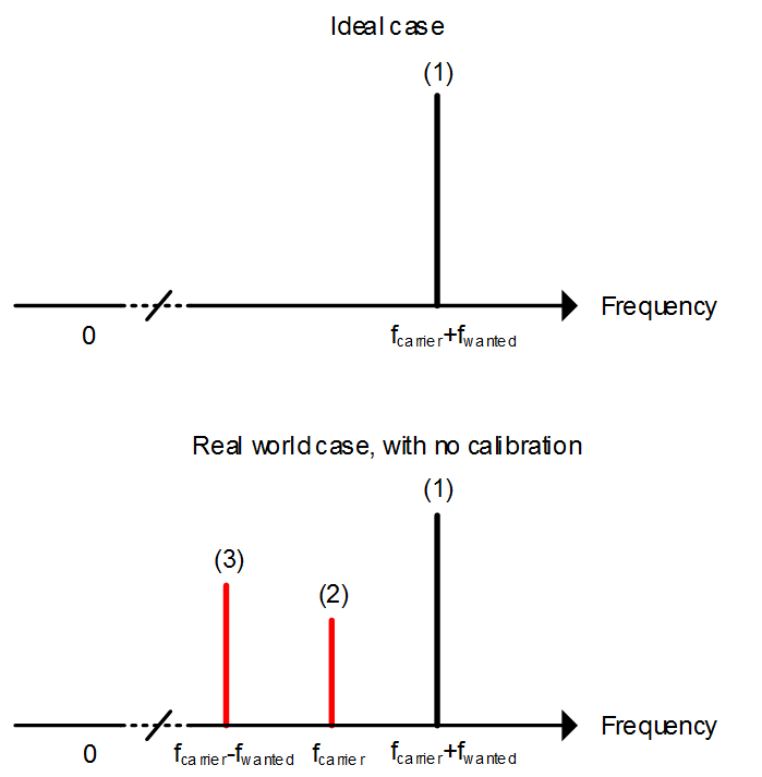
For the ideal TX case, if the continuous wave (CW) signal is up-converted to radio frequency (RF), the TX output ideal spectrum has no unwanted components, as shown in Figure 1 upper graph. In non-linear conditions, the TX output spectrum has unwanted tones as shown in Figure 1 lower graph. Descriptions of the tones are given below:
- Wanted Signal (1) – wanted TX sideband, with an offset fwanted from the carrier frequency fcarier;
- LO Leakage (2) – primarily caused by DC offsets in the TX baseband and LO leakage at the TX frequency mixing stage;
- IQ Image (3) – unwanted TX sideband, with an offset -fwanted from the carrier frequency fcarier. Primary caused by gain and phase imbalances in different IQ signal blocks.

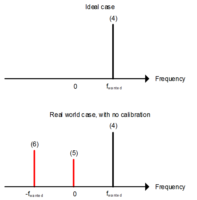
For the ideal RX case, the down-converted CW signal does not have unwanted tones at the input of the analog-digital-converter (ADC) as shown in the Figure 2 upper graph. However, under non-linear conditions the RX spectrum has unwanted signals as shown in the Figure 2 lower graph. Descriptions of the tones are given below:
- Wanted Signal (4) – wanted RX sideband, with an offset fwanted from the DC;
- DC Offset (5) – Unwanted RX DC offset. Primarily caused by DC offsets in the RX baseband and LO leakage at the RX frequency mixing stage;
- IQ Image (6) – Unwanted RX sideband, with an offset -fwanted from the DC. Primary caused by gain and phase imbalances in different quadrature (IQ) signal blocks.
Calibration procedure 1 is used to calibrate unwanted tones. The goal of the MCU program executing the calibration procedure is to find suitable LMS7002M DC offset, gain or phase correction control values for TX and RX, at which the unwanted tones are reduced to levels close to ideal cases shown in Figure 1 and Figure 2.

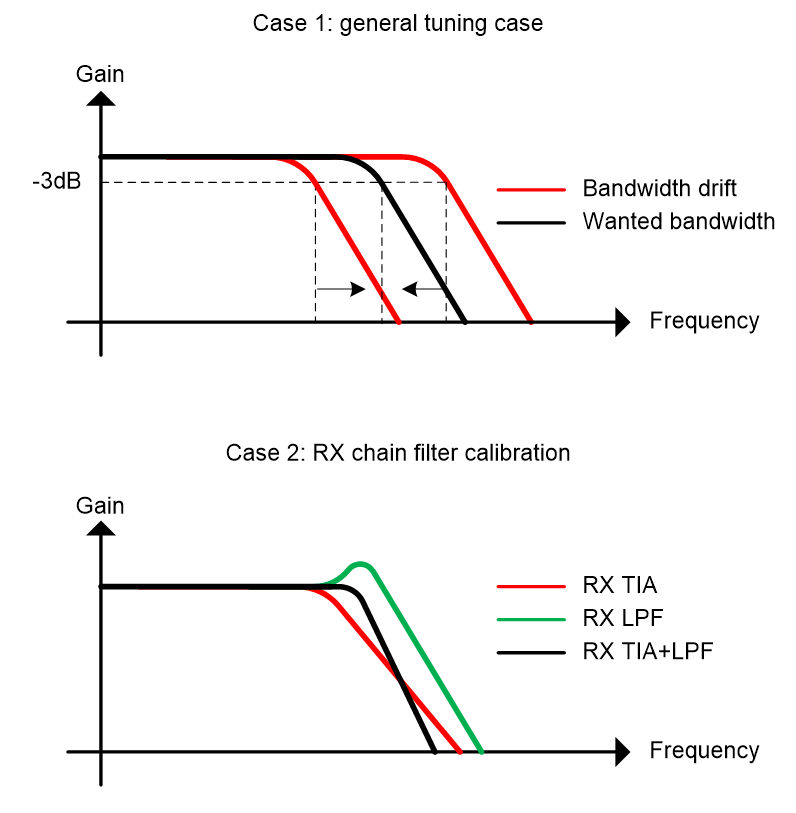
Calibration procedure 2 is used for analog filter bandwidth calibration. The procedure can be used to tune the desired filter(s) to a new bandwidth setting or to perform re-calibration on an active setup. Figure 3 shows two cases of analog filter tuning:
- Case 1 – General case. Filter -3dB bandwidth is tuned to a particular frequency or re-calibrated for a new setup;
- Case 2 – Multiple filter stage tuning. On RX side, the transpimedance amplifier (TIA) acts as a 1st order low pass filter (LPF), while the baseband LPF provides a 2nd order Chebyshev response with a 3 dB peak. Combining both filters can yield a 3rd order LPF with a tunable in-band response. Both stages need to be calibrated separately to produce the desired filter response. A similar setup is used in the TX low band stage.
The MCU program automatically selects the appropriate analog filter bandwidth calibration case in respect to the wanted bandwidth. It also handles the appropriate power down (PD) or enable (EN) controls of the involved blocks (manual setup is not needed).

General MCU calibration limitations and options
The internal LMS7002M MCU has 16384 bytes of memory, thus the size of the calibration program is limited. Furthermore, it takes time (further elaborated in Section 2) to program the MCU, hence only the main (used most frequently) calibration procedures (see Section 1.1) are stored in the MCU image. Other calibration procedures, such as PLL frequency, TX gain tuning, should be implemented as separate baseband processor routines and should be ported separately using the latest source code found on LimeSuite GitHub webpage. Thus, time for MCU image upload is reduced and the overall calibration speed is increased.
By default, MCU calibration image uses internal LMS7002M RF loopback to perform the required test signal generation procedures, hence no external components or connections are required. Nonetheless, internal RF loopback has bandwidth and signal coupling limitations. It achieves the best calibration performance up to 2GHz, but can be effectively used up to 2.7GHz (where unwanted tone suppression will decrease down to <−35dBc). External RF loopback can be used to remove the RF limitation, but this requires a modification on the board level and the use of a separate MCU image (based around the particular board). Please note, that only DC offset, LO leakage, gain and phase mismatch calibration procedures are affected by the internal/external loopback selection, while other calibration routines do not depend on board connection modifications.
Use of MCU Calibration Image
General Information
LMS7002M MCU image calibration procedures
MCU calibration image (see Section 2.1.2) has the following calibration routines that can be executed:
- Calibration of TX chain DC offset and LO leakage, phase, gain imbalances;
- Calibration of RX chain DC offset, phase, gain imbalances;
- Calibration of TX analog filter bandwidth;
- Calibration of RX analog filter bandwidth.
Other data handling procedures (for example certain variable input to the MCU) will be discussed in Section 2.2.
LMS7002M Setup Steps Needed for MCU Image Calibration Execution
LMS7002M IC must be properly set-up from the stand-point of analog and digital interface settings prior to main DC offset and LO, phase, gain calibration procedures handled by the MCU image for both TX and RX chains.
The recommended calibration/tuning priority list for TX chain is given below:
- TX and clock generator (CLKGEN) PLL frequency tuning (block order is irrelevant, baseband processor routine, see Section 1.2);
- TX analog filter bandwidth (handled by the MCU image);
- TX gain tuning (baseband processor routine, see Section 1.2);
- Settings of other TX chain controls (bias, power amplifier gain and etc.). Please note, that digital interface speed should also be configured at this or any of the earlier stages;
- TX DC offset and LO, phase gain calibration (handled by the MCU image).
The recommended calibration/tuning priority list for RX chain is given below:
- RX and clock generator (CLKGEN) PLL frequency tuning (block order is irrelevant, baseband processor routine, see Section 1.2);
- RX analog filter bandwidth (handled by the MCU image);
- Settings of other RX chain controls (bias, LNA, TIA, PGA gain and etc.). Please note, that digital interface speed should also be configured at this or any of the earlier stages;
- RX DC offset and LO, phase gain calibration (handled by the MCU image).
MCU calibration can handle a single procedure at a given time – calibrating both A and B channels or executing several calibrations procedures simultaneously at the same time is not possible. MCU calibrates only currently selected transceiver channel, which is selected by SPI 0x0020[1:0] bits. Baseband has to select channel and initiate calibration for each transceiver channel individually.
MCU Calibration Image Location
The latest MCU calibration image can always be found on LimeSuie GitHub webpage:
MCU Internal Memory Size
MCU internal memory size is 16384 bytes. It is required that all 16384 bytes have to be uploaded before the MCU becomes programmed. If program image size is less than 16384 bytes, image should be padded with zeros to meet the required size.
MCU Programming Information
Programming the MCU
- Reset MCU, write to SPI address 0x0002 = 0;
- Set one of the programming modes:
- EEPROM and SRAM, write to SPI address 0x0002 = 1;
- SRAM, write to SPI address 0x0002 = 2;
- Wait until MCU programming buffer is empty, read from SPI address 0x0003[0]:
- 0x0003[0] == 0, buffer empty;
- 0x0003[0] == 1, buffer has data;
- Write 32 bytes of program image into MCU buffer, by SPI writing to address 0x0004;
- Go to step 3. until 16384 total bytes have been written;
- Wait until MCU becomes programmed, read from SPI address 0x0003[6]:
- 0x0003[6] == 0, MCU not programmed;
- 0x0003[6] == 1, MCU programmed.
Running MCU Image Calibration Procedure
The following steps are needed to run the MCU image calibration procedure:
- SPI write 0x0006[0] = 1, switch SPI controls to MCU;
- SPI write 0x0000 = procedure ID (see Table 1);
- SPI write 0x0002[3] = 0;
- SPI write 0x0002[3] = 1;
- SPI write 0x0002[3] = 0;
- SPI read address 0x0001;
- IF 0x0001== 0xFF, MCU procedure is in progress, repeat step 6;
- IF 0x0001== 0, MCU procedure finished successfully;
- IF 0x0001== Any Other Value, MCU encountered error;
- SPI write 0x0006[0]=0, switch SPI controls back to baseband.