Lime-GPSDO v1.0 hardware description: Difference between revisions
(→GPIO) |
|||
| Line 183: | Line 183: | ||
{| class="wikitable" | {| class="wikitable" | ||
|+ Table | |+ Table 3. GPIO connection | ||
! Connector pin !! Schematic signal name !! FPGA pin !! FPGA I/O standard !! Comment | ! Connector pin !! Schematic signal name !! FPGA pin !! FPGA I/O standard !! Comment | ||
|- | |- | ||
Revision as of 11:52, 11 April 2019
Lime-GPSDO Board Key Features
The Lime-GPSDO development board provides high stability clock source for timing sensitive applications. Clock frequency is being constantly monitored inside MAX10 FPGA and tuned by PPS signal from GNSS module.
For more information on the following topics, refer to the respective documents:
Lime-GPSDO board features:
- USB Interface
- Silicon labs USBXpress Family USB-to-UART bridge CP2102N.
- FPGA Features
- MAX10 10M16SAU169C8 device in 169-pin UBGA
- 16K logic elements
- 549 Kbits embedded memory (M9K) and 2368 Kbits of user Flash Memory
- 45 embedded 18x18 multipliers
- 1 PLLs
- FPGA Configuration
- JTAG mode configuration
- Memory Devices
- 4Mbit FLASH
- 128Kbit (16K x 8) EEPROM
- Connections
- microUSB2.0 (type B)
- SMA connectors for clock IN/OUT, time pulse output and GNSS antenna
- FPGA GPIO header (0.05” pitch)
- FPGA JTAG connectors (0.05” pitch and side connector)
- 5V DC power jack and pinheader
- Backup battery connector for GNSS receiver
- Clock output pinheader
- External UART connector
- External I2C connector
- Clock System
- 30.72MHz VCOCXO:
- Frequency calibration ±0.5ppm;
- Frequency stability over temperature in still air ±20ppb;
- Frequency slope ΔF/ΔT in still air ±1.2ppb/°C
- Possibility to tune VCOCXO by onboard DAC
- Possibility to use GNSS PPS signal as a reference when tuning VCOCXO frequency
- 30.72MHz VCOCXO:
- Board Size without connectors 50.50mm x 80mm (1.99” x 3.15”)
Board Overview
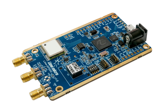
Lime-GPSDO board version 1.0 picture with highlighted major components and connections presented in Figure 1 and Figure 2. There are three connector types – data and debugging (USB2.0, FPGA GPIO and JTAG), power (DC jack and external supply pinheader), clock source output, GNSS antenna and time pulse output.
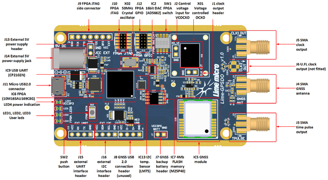
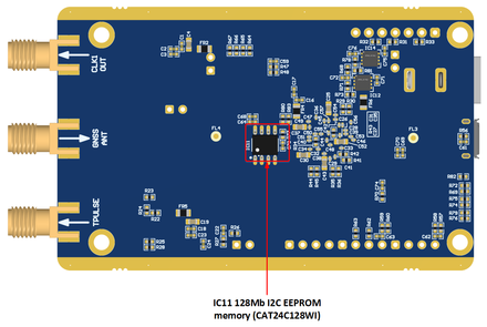
Board components description listed in the Table 1 and Table 2.
| Featured Devices | ||
|---|---|---|
| Board reference | Type | Description |
| IC5 | GNSS module | GNSS receiver |
| IC5 | FPGA | Intel MAX 10 (10M16SAU169C8G 169-UBGA) |
| IC9 | USB UART | Silicon labs USB-to-UART bridge |
| Miscellaneous devices onboard | ||
| IC13 | IC | Temperature sensor LM75 |
| Configuration, Status and Setup Components | ||
| J9 | JTAG chain pin header | FPGA programming pin header for Altera USB-Blaster download cable, side connection. |
| J10 | JTAG chain pin header | FPGA programming pin header for Altera USB-Blaster download cable, 0.05” pitch |
| LEDS1, LEDS2, LEDS3 | Red-green status LEDs | User defined FPGA indication. |
| General User Input/Output | ||
| J12 | Pin header | 8 FPGA GPIOs plus 2 power pins, 0.05” pitch |
| SW1 | Slide switch | 4 slide switches connected to FPGA |
| SW2 | Push button | Push button connected to FPGA |
| Memory Devices | ||
| IC11 | EEPROM | 128K (16K x 8) EEPROM connected to FPGA |
| IC10 | IC | I²C EEPROM Memory 128Kb (16K x 8), connected to FPGA I2C bus |
| IC7 | Flash memory | 4Mbit FLASH memory connected to FPGA |
| Communication Ports | ||
| J11 | USB2.0 connector | microUSB2.0 (type B) connector |
| J8 | Header | GNSS USB 2.0 connection header (unused) |
| J15 | Header | External UART interface header, can be used to control external periphery. Additional logic has to be implemented in FPGA. |
| J16 | Header | External I2C interface header, can be used to control external periphery. Additional logic has to be implemented in FPGA. |
| Clock Circuitry | ||
| XO1 | VCOCXO | 30.72MHz voltage-controlled crystal oscillator used as a reference clock. |
| XO2 | XO | 50MHz crystal oscillator, used for FPGA logic. |
| IC2 | DAC | Analog devices 16bit Digital-to-analog converter for VCOCXO voltage control |
| J1 | Pin header | Optional clock output of XO1 |
| J2 | Pin header | Optional Voltage control input for XO1 |
| J3 | SMA connector | Time pulse output from GNSS modules |
| J5 | SMA connector | Reference clock output |
| J6 | U.FL connector | Reference clock output, connector is not fitted by default. |
| Power Supply | ||
| J14 | DC input jack | External 5V DC power supply |
| J13 | Pin header | External 5V DC power supply and main internal power rail |
| Other | ||
| J4 | SMA connector | Antenna input for GNSS module |
| J7 | Pin header | Backup battery connection header for GNSS module. Typical 3.0V (follow recommendation in fitted GNSS module datasheet) |
LimeSDR-Mini Board Architecture
The heart of the Lime-GPSDO board is Intel MAX10 FPGA. Its main function is to measure VCOCXO clock frequency and tune it by PPS signal from GNSS module and provide control. The block diagram for Lime-GPSDO board is presented in the Figure 3.
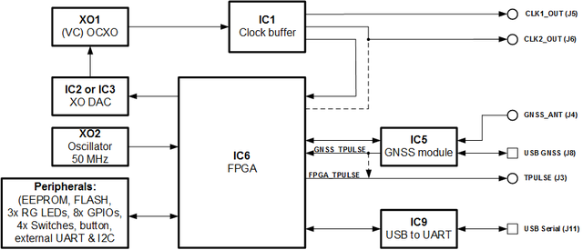
GNSS module
GNSS module has serial data communication interface, timing pulse and other control signals connected to FPGA. It also has SMA connector for external antenna.
| Chip pin (IC5) | Chip reference (IC5) | Schematic signal name | FPGA pin | FPGA I/O standard | Comment |
|---|---|---|---|---|---|
| 3 | TIMEPULSE | GNSS_TPULSE | A2 | 3.3-V LVCMOS | Also connected to J3 SMA conn. |
| 4 | EXTINT | GNSS_EXTINT | B1 | 3.3-V LVCMOS | |
| 8 | RESET_N | GNSS_RESET | C1 | 3.3-V LVCMOS | |
| 14 | LNA_EN /RESV | GNSS_OFF | F1 | 3.3-V LVCMOS | |
| 15 | RTK_STAT /RESV | GNSS_ANT_DET | E1 | 3.3-V LVCMOS | |
| 16 | GEOFENCE_STAT /RESV | GNSS_ANT_OK | D1 | 3.3-V LVCMOS | |
| 18 | DDC_SDA /SPI_CSN | GNSS_DDC_SDA | B2 | 3.3-V LVCMOS | |
| 19 | DDC_SCL /SPI_CLK | GNSS_DDC_SCL | A3 | 3.3-V LVCMOS | |
| 20 | UART_TX /SPI_MISO | GNSS_UART_TX | B3 | 3.3-V LVCMOS | |
| 21 | UART_RX /SPI_MOSI | GNSS_UART_RX | A4 | 3.3-V LVCMOS | |
| 11 | RF_IN | RF_IN | - | - | Connected to J4 SMA conn. |
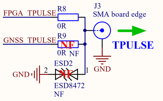
By default time pulse output (J3 SMA connector) is connected to FPGA pin C2 output but can be changed to GNSS time pulse signal by removing R8 resistor and soldering R9 resistors. Refer to Figure 4.
GPIO
There are eight general purpose input/output pins from FPGA connected to FPGA GPIO header (J12). Schematic names and pin connections can be found in Table 4.
| Connector pin | Schematic signal name | FPGA pin | FPGA I/O standard | Comment |
|---|---|---|---|---|
| 1 | FPGA_GPIO0 | M12 | 3.3V | |
| 2 | FPGA_GPIO1 | M10 | 3.3V | |
| 3 | FPGA_GPIO2 | N12 | 3.3V | |
| 4 | FPGA_GPIO3 | N10 | 3.3V | |
| 5 | FPGA_GPIO4 | M11 | 3.3V | |
| 6 | FPGA_GPIO5 | M9 | 3.3V | |
| 7 | FPGA_GPIO6 | N11 | 3.3V | |
| 8 | FPGA_GPIO7 | N9 | 3.3V | |
| 9 | GND | - | ||
| 10 | VCC | - | 3.3V or 5V selectable power rail. |
Voltage for pin 10 of J12 connector can be 3.3V (default) or 5V. To connect this pin to 5V power rail remove R47 and solder R48 resistors (see Figure 5).
Indication LEDs
Lime-GPSDO board comes with four dual color (red and green (RG)) indication LEDs. Most of LEDs are connected to FPGA and their function can be changed. Default LEDs functions and other information are listed in the table below.
| Board Reference | Schematic signal name | Board label | FPGA pin | Description |
|---|---|---|---|---|
| LED1 | FPGA_LED1_G | LED1 | A11 | GNSS lock and VCOCXO tune state: Solid RED – no GPS lock; Blinking RED – GPS is locked, 1s lowest accuracy tune state; Blinking RED/GREEN - GPS is locked, 10s accuracy tune state; Blinking GREEN - GPS is locked, 100s highest accuracy tune state. |
| FPGA_LED1_R | B11 | |||
| LED2 | FPGA_LED2_G | LED2 | A10 | |
| FPGA_LED2_R | B10 | |||
| LED3 | FPGA_LED3_G | LED3 | A8 | |
| FPGA_LED3_R | A9 | |||
| LED4 | - | LED4 VCC3P3 | - | Green LED indicates VCC3P3 power rail presence. Red LED is unused |
| - | - |
Switch and push button
There are four sliding switches and one push button connected to FPGA. Sliding switch to “ON” position sets logic “0” level and opposite sets logic “1”. Default functions and connection information are listed in the table below.
| Board Reference | Schematic signal name | Board label | FPGA pin | Description |
|---|---|---|---|---|
| SW1 | FPGA_SW0 | FPGA SWITCH | N7 | FPGA_SW[1:0]=x0 - UART of GNNSS module connected to USB UART FPGA_SW[1:0]= 01 - limegnss_gpio module connected to USB UART |
| FPGA_SW1 | M7 | |||
| FPGA_SW2 | N8 | Not used | ||
| FPGA_SW3 | M8 | Not used | ||
| SW2 | FPGA_BTN | FPGA BTN | B7 | Board reset |
Communication interfaces
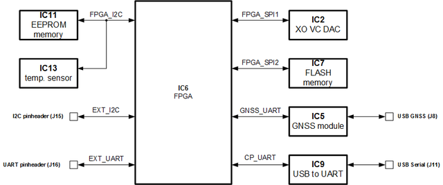
Lime-GPSDO board has various options of communication interfaces. There is USB-to-UART bridge and micro USB connector, pin headers for UART, I2C and interfaces for onboard periphery. For graphical representation see Figure 6 and detailed description can be found in Table 7.
| Schematic signal name | FPGA pin | I/O standard | Comment |
|---|---|---|---|
| FPGA_I2C_SCL | J1 | 3.3V | Serial Clock |
| FPGA_I2C_SDA | K1 | 3.3V | Data |
| EXT_I2C_SCL | B4 | 3.3V | Serial Clock |
| EXT_I2C_SDA | A5 | 3.3V | Data |
| FPGA_SPI1_SCLK | N5 | 3.3V | Serial Clock (FPGA output) |
| FPGA_SPI1_MOSI | N4 | 3.3V | Data, master output |
| FPGA_SPI1_DAC_SS | N6 | 3.3V | Slave select |
| FPGA_SPI2_SCLK | M4 | 3.3V | Serial Clock (FPGA output) |
| FPGA_SPI2_MOSI | N3 | 3.3V | Data, master output |
| FPGA_SPI2_FLASH_SS | N2 | 3.3V | Slave select |
| GNSS_UART_TX | B3 | 3.3V | GNSS UART transmit (FPGA input) |
| GNSS_UART_RX | A4 | 3.3V | GNSS UART receive (FPGA output) |
| CP_CTS | F13 | 3.3V | Clear To Send control input (FPGA output) |
| CP_RTS | F12 | 3.3V | Ready To Send control output (FPGA input) |
| CP_RXD | G13 | 3.3V | Asynchronous data input (FPGA output) |
| CP_TXD | G12 | 3.3V | Asynchronous data output (FPGA input) |
| CP_DSR | H13 | 3.3V | Data Set Ready control input (FPGA output) |
| CP_DTR | J13 | 3.3V | Data Terminal Ready control output (FPGA input) |
| EXT_UART_RX | C12 | 3.3V | UART receive |
| EXT_UART_TX | C11 | 3.3V | UART transmit |
Temperature sensor
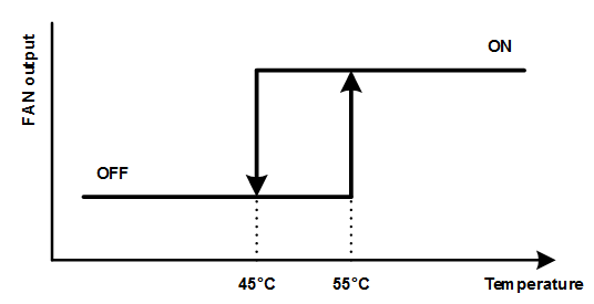
Lime-GPSDO has integrated temperature sensor which can be used to monitor board temperature through I2C interface.
Sensor has overtemperature shutdown output connected to FPGA. Which can be used to take actions to reduce board temperature when it rises below set limits. For example, fan will be turned on if board will heat up to 55°C and FAN will be turned off if board will cool down to 45°C.
| Schematic signal name | FPGA pin | I/O standard | Comment |
|---|---|---|---|
| FPGA_I2C_SCL | J1 | 3.3V | Serial Clock |
| FPGA_I2C_SDA | K1 | 3.3V | Data |
| LM75_OS | H1 | 3.3V | Overtemperature shutdown output (FPGA input) |
Clock Distribution
Lime-GPSDO board has onboard 30.72 MHz VCOCXO that is reference clock output. Clock distribution block diagram is presented in Figure 8.
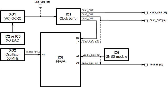
VCOCXO frequency can be tuned by DAC (IC2). There is voltage control input of VCOCXO exposed and connected to J2 pin header. By removing R10 resistor and providing control voltage trough J2 header VCOCXO frequency can be tuned externally. Refer to XO1 Rakon U7475LF datasheet for valid control voltage ranges.
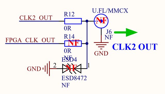
J6 SMA connector source can be changed from IC1 clock buffer (default configuration) to FPGA (IC6) clock output by removing R12 and fitting R14 resistors. Refer to Figure 9.
