LimeNET-Micro v2.1 hardware description: Difference between revisions
| Line 337: | Line 337: | ||
| Fan connection header | | Fan connection header | ||
|} | |} | ||
== LimeNET-Micro board architecture == | |||
Revision as of 16:52, 19 March 2019
LimeNET-Micro Board Key Features
LimeNET Micro makes deploying wireless networks more accessible than ever before, by extending the LimeNET line of integrated hardware solutions via an ultra-low cost platform that is capable of supporting narrowband systems, such as GSM and IoT wireless standards, in a stand-alone configuration.
LimeNET-Micro board features:
- RF transceiver
- Lime Microsystems LMS7002M
- Raspberry Pi
- DDR2 SODIMM socket for raspberry Pi CM3(L)
- 2x downstream USB 2.0 ports
- Upstream Micro-USB for USB boot of Compute Module
- 3.5mm analog audio, composite video output
- Ethernet + active PoE (RJ45) connector
- Ribbon cable camera and display connectors
- HDMI connector
- External UART connector
- uSD card slot
- USB2.0 HUB and 10/100 Ethernet controller
- SDIO Wi-Fi module
- Jumper for Raspberry boot mode selection
- FPGA Features
- Intel MAX10 10M16SAU169C8 device in 169-pin UBGA
- 16K logic elements
- 549 Kbits embedded memory (M9K) and 2368 Kbits of user Flash Memory
- 45 embedded 18x18 multipliers
- 1 PLLs
- FPGA Configuration
- JTAG mode configuration
- USB Controller
- FTDI FT601 USB to FIFO interface bridge chip (connects FPGA to USB2.0 HUB)
- Memory Devices
- 4Mbit FLASH (for FPGA data)
- 2x 128Kbit (16K x 8) EEPROM (for LMS MCU firmware and FPGA data)
- Other Devices
- Temperature sensor
- Crypto Authentication Device
- GNSS receiver
- Connections
- 2 x coaxial RF (SMA) connectors
- SMA connectors for reference clock IN/OUT, GNSS and Wi-Fi antennas
- 5V DC power jack
- 5V header for powering external devices
- Fan header
- FPGA JTAG connectors (0.05” pitch and side connector)
- Backup battery connector for GNSS receiver
- Clock System
- 30.72MHz VCOCXO:
- Frequency calibration ±0.5ppm;
- Frequency stability over temperature in still air ±20ppb;
- Frequency slope ΔF/ΔT in still air ±1.2ppb/°C
- Possibility to tune VCOCXO by onboard DAC
- Possibility to use GNSS PPS signal as a reference when tuning VCOCXO frequency
- 30.72MHz VCOCXO:
- User I/O
- GPIO header (0.05” pitch) connected to FPGA
- 5X dual color (RG) LEDs connected to FPGA
- Push button connected to FPGA
- Buzzer connected to FPGA
- Board Size: without connectors 125mm x 65mm (4.92” x 2.56”)
For more information on the following topics, refer to the respective documents:
- FT601 controller resources [link]
- MAX10 device family, refer to Intel documentation [link]
- LMS7002M transceiver resources [link]
Board Overview
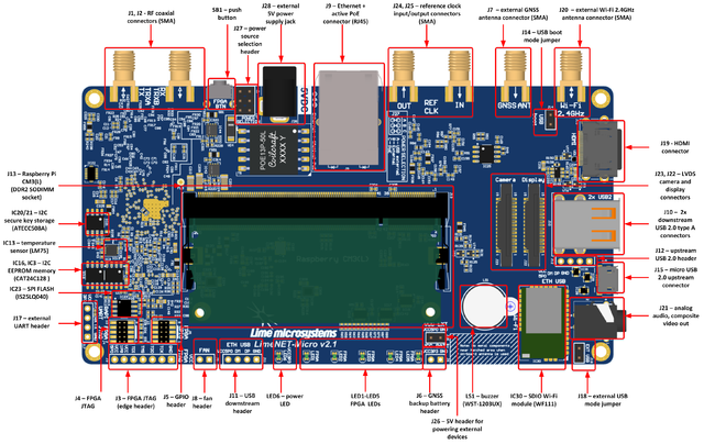
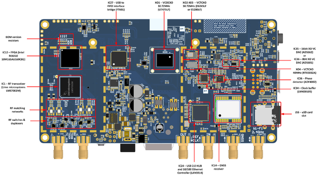
LimeNET-Micro board version 2.1 picture with highlighted major components and connections presented in Figure 1 and Figure 2. Lime Microsystems LMS7002M RF transceiver and Intel MAX10 FPGA can be found on bottom side of board, DDR2 SODIMM socket for Raspberry PI Compute module is placed on top side. There are three connector types – data and debugging (USB2.0, FPGA GPIO, Ethernet and JTAG), power (DC jack and external supply pinheader), RF (clock source output, GNSS antenna and time pulse output, RF transmit and receive ports). LimeNET-Micro 2.1 board comes in three versions and each version differs in components which are fitted on board (BOM – Bill Of Material). BOM version can be determined from resistors R34, R35, R36, R37 fitted on board (see Figure 2 “BOM version resistors” and Table 1 for version description).
| BOM_VER | R34 | R35 | R36 | R37 | Comment |
|---|---|---|---|---|---|
| 0 | Fitted | Fitted | Fitted | Fitted | Lime (full version) |
| 1 | NF | Fitted | Fitted | Fitted | SDR (without duplexers and WiFi module) |
| 2 | Fitted | NF | Fitted | Fitted | GSM (with duplexers, without PoE, audio and video) |


Board components description listed in the Table 2 and Table 3.
| Featured devices | ||
|---|---|---|
| Board Reference | Type | Description |
| IC1 | RF transceiver | Lime Microsystems LMS7002M |
| IC14 | GNSS module | GNSS receiver |
| IC12 | FPGA | Intel MAX10, 10M16SAU169C8G, 169-UBGA |
| IC24 | USB 2.0 HUB | Microchip Technology LAN9514 USB 2.0 Hub and 10/100 Ethernet Controller |
| IC27 | USB to FIFO | FTDI FT601, USB to FIFO interface bridge |
| IC30 | Wi-Fi | SDIO Wi-Fi module (WF111) |
| Miscellaneous devices onboard | ||
| IC13 | IC | Temperature sensor LM75 |
| IC20/21 | IC | I2C secure key storage ATECC508A |
| Configuration, Status and Setup Elements | ||
| J3 | JTAG chain pin header | FPGA programming pin header for Altera USB-Blaster download cable, side connection. |
| J4 | JTAG chain pin header | FPGA programming pin header for Altera USB-Blaster download cable, 0.05” pitch |
| LED1,
LED2, LED3, LED4, LED5 |
Red-green status LEDs | User defined FPGA indication. |
| LED6 | Red-green status LEDs | VCC3P3 power rail indications |
| LS1 | Buzzer | Buzzer (WST-1203UX), connected to FPGA. |
| J14 | Jumper | USB boot mode jumper |
| J18 | Jumper | External USB mode jumper |
| J27 | Jumper | Power source selection |
| General User Input/Output | ||
| J5 | Pin header | 8 FPGA GPIOs plus 2 power pins, 0.05” pitch |
| SB1 | Push button | Push button connected to FPGA |
| Memory Devices | ||
| IC3, IC16 | EEPROM | 128K (16K x 8) EEPROM connected to FPGA and LMS7002M |
| IC23 | Flash memory | 4Mbit FLASH memory connected to FPGA |
| Communication Ports and interfaces | ||
| J9 | RJ45 connector | Ethernet + active PoE connector |
| J10 | USB2.0 connector | 2x downstream USB2.0 type A connectors |
| J11 | Header | USB downstream header |
| J12 | Header | Upstream USB2.0 header |
| J13 | Socket | DDR2 SODIMM socket for Raspberry Pi CM3(L) |
| J15 | USB2.0 connector | microUSB2.0 upstream connector |
| J17 | Header | External UART header |
| J19 | Connector | HDMI connector for display |
| J22 | Connector | LVDS connector for display |
| J23 | Connector | LVDS connector for camera |
| Clock Circuitry | ||
|---|---|---|
| Board Reference | Type | Description |
| XO1 | VCOCXO | 30.72 MHz voltage-controlled crystal oscillator used as a reference clock. |
| XO2 | VCTCXO | 30.72 MHz voltage-controlled, temperature compensated crystal oscillator used as a reference clock. |
| XO3 | VCTCXO | 30.72 MHz voltage-controlled, temperature compensated crystal oscillator used as a reference clock. (Not fitted by default) |
| XO4 | VCTCXO | 40.0 MHz voltage-controlled, temperature compensated crystal oscillator used as a reference clock. |
| IC35 OR IC37 | IC | Analog devices 16bit AD5662 or 8bit AD5601 Digital-to-analog converter for reference clock voltage control |
| IC36 | IC | Phase detector (ADF4002) |
| J25 | SMA connector | Reference clock input |
| J24 | SMA connector | Reference clock output |
| RF connectors | ||
| J1 | SMA connector | Transmit port or TRXA channel in duplex mode |
| J2 | SMA connector | Receive port or TRXB channel in duplex mode |
| J7 | SMA connector | GNSS module antenna connector |
| J20 | SMA connector | Antenna connector for Wi-Fi module |
| Power Supply | ||
| J28 | DC input jack | External 5V DC power supply input |
| J26 | Pin header | 5V DC power supply output header and main internal power rail |
| J6 | Pin header | Backup battery connection header for GNSS module. Typical 3.0V (follow recommendation in fitted GNSS module datasheet) |
| Other | ||
| J16 | Card slot | uSD card slot for Raspberry Pi boot |
| J11 | Header | Fan connection header |