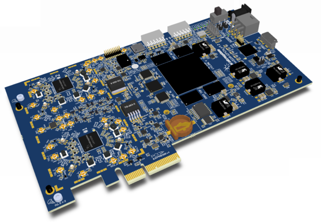
LimeSDR-QPCIe v1.2 hardware description: Difference between revisions
| Line 78: | Line 78: | ||
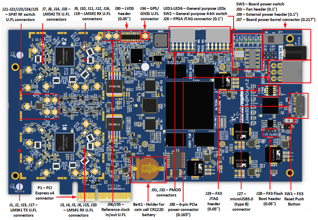
LimeSDR-QPCIe board version 1.2 picture with highlighted major connectors presented in Figure 2. There are three connector types – data and debugging (PCIe, USB3.0, PMOD, LVDS and JTAG), power (DC jack and external supply pinheaders) and high frequency (RF and reference clock). | LimeSDR-QPCIe board version 1.2 picture with highlighted major connectors presented in Figure 2. There are three connector types – data and debugging (PCIe, USB3.0, PMOD, LVDS and JTAG), power (DC jack and external supply pinheaders) and high frequency (RF and reference clock). | ||
[[File:LimeSDR-QPCIe_v1.2_Development_Board_Connectors.png|thumb|center|640px|Figure 2 LimeSDR-QPCIe v1.2 Development Board Connectors]] | |||
Figure 2 LimeSDR-QPCIe v1.2 Development Board Connectors | |||
Board components description listed in the Table 1 and Table 2. | Board components description listed in the Table 1 and Table 2. | ||
////////////////INSERT TABLES | |||
LimeSDR-QPCIe board version 1.2 picture with highlighted top components are presented in Figure 3. | |||
[[File:LimeSDR-QPCIe_Development_Board_Top_Components.png|thumb|center|640px|Figure 3 LimeSDR-QPCIe Development Board Top Components]] | |||
LimeSDR-QPCIe board version 1.2 picture with highlighted bottom components is presented in Figure 4. | |||
[[File:LimeSDR-QPCIe_Development_Board_Bottom_Components.png|thumb|center|640px|Figure 4 LimeSDR-QPCIe Development Board Bottom Components]] | |||
Revision as of 12:46, 24 May 2018
Introduction
LimeSDR-QPCIe is low-cost software defined radio board based on Lime LMS7002M Field Programmable Radio Frequency (FPRF) transceiver and Altera Cyclone V PFGA, through which apps can be programmed to support any type of wireless standard, e.g. UMTS, LTE, LoRa, GPS, WiFi, Zigbee, RFID, Digital Broadcastimng, Radar and many more.
LimeSDR-QPCIe Board Key Features
The LimeSDR-QPCIe development board provides a hardware platform for developing and prototyping high-performance and logic-intensive digital and RF designs using Altera’s Cyclone V FPGA and Lime Microsystems transceiver.

For more information on the following topics, refer to the respective documents:
- Cyclone V device family, refer to Cyclone V Device support resources link
- LMS7002M transceiver resources link
LimeSDR-QPCIe v1.2 board features:
- USB Interface
- Cypress FX3 Super Speed USB 3rd generation controller
- FPGA Features
- Cyclone V, 5CGXFC7D7F31C8N device in 896-pin FBGA package
- 150’000 logic elements
- 6860 Kbits embedded memory
- 312 embedded 18x18 multipliers
- 7 PLLs
- 9 Transceivers (2.5Gbps)
- PCIe Hard IP Blocks
- 2 Hard Memory Controllers
- FPGA Configuration
- JTAG mode configuration
- Active serial mode configuration
- Possibility to update FPGA gateware by using FX3 (USB)
- Possibility to update FPGA gateware by using PCIe interface.
- RF
- 2x LMS7002M, FPRF transceivers
- Onboard RSSI measurement circuits
- Onboard loopback control switches
- DACs and ADCs
- 2x DAC5672A, dual, 14-bit, Digital-To-Analog converters
- 1x ADS424, Dual-Channel, 14-bit, Analog-To-Digital converter
- Memory Devices
- 4 x 2Gbit DDR3 SDRAM (128M x 16)
- 4Mbit flash for FX3 firmware
- 128Mbit flash for FPGA gateware
- 2 x 128Kbit and 2 x 512Kbit EEPROMs for LMS MCU firmware, LMS MCU data
- 1 x 128K EEPROM for FX3 or FPGA data
- Connections
- microUSB3.0 (type B) connector
- PCIe x4 edge connector (Gen1)
- Coaxial RF (U.FL) connectors
- 2x PMOD header (0.1” pitch)
- FPGA (0.1” pitch) and FX3 (0.05” pitch) JTAG connectors
- 12V DC power jack and pinheader
- LVDS connector (0.05” pitch)
- Fan connector (12V/5V)
- PCIe 6-pin power connector
- Holder for coin cell CR1220 battery
- Clock System
- 30.72MHz VCTCXO (precision: ±1 ppm initial, ±4 ppm stable).
- Possibility to lock VCTCXO to external clock using ADF4002 or tune VCTCXO by onboard DAC (AD5662)
- Programmable clock generator for the FPGA reference clock input or LMS PLLs
- VCTCXO clock output for external device synchronization.
- 1x 100 MHz, 4 x 125MHz crystal oscillators for FPGA
- Miscellaneous devices
- LM75 Digital temperature sensor with 2-Wire Interface.
- DS3231 real-time clock.
- M0578-A3 GPS/GNSS module receiver
- Board Size 190mm x 106.7mm (7.48” x 4.20”)
LimeSDR-QPCIe Board Overview
LimeSDR-QPCIe board version 1.2 picture with highlighted major connectors presented in Figure 2. There are three connector types – data and debugging (PCIe, USB3.0, PMOD, LVDS and JTAG), power (DC jack and external supply pinheaders) and high frequency (RF and reference clock).

Board components description listed in the Table 1 and Table 2.
////////////////INSERT TABLES
LimeSDR-QPCIe board version 1.2 picture with highlighted top components are presented in Figure 3.
LimeSDR-QPCIe board version 1.2 picture with highlighted bottom components is presented in Figure 4.