LimeSDR-PCIe FPGA programming: Difference between revisions
| Line 142: | Line 142: | ||
*Click Hardware Setup.. button and select your download cable, click Close (see Figure 46). | *Click Hardware Setup.. button and select your download cable, click Close (see Figure 46). | ||
Figure | [[File:LimeSDR-PCIe_FPGA_selecting_prog.png|thumb|center|640px|Figure x. Selecting programming hardware]] | ||
*Click Add File.. and select *.jic file (see options below): | *Click Add File.. and select *.jic file (see options below): | ||
| Line 150: | Line 151: | ||
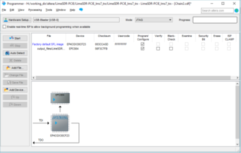
*Apply settings as in Figure 47 and click Start. | *Apply settings as in Figure 47 and click Start. | ||
Figure | [[File:LimeSDR-PCIe_FPGA_adding_prog_file.png|thumb|center|640px|Figure x. Adding programming file]] | ||
*After successful programming turn off computer #1. | *After successful programming turn off computer #1. | ||
*FPGA boots from programmed FLASH memory automatically when computer #1 is turned on. | *FPGA boots from programmed FLASH memory automatically when computer #1 is turned on. | ||
Revision as of 09:04, 1 March 2018
Draft
FPGA gateware programming
This chapter describes steps to program LimeSDR-PCIe board. If you already have valid programming *.jic file skip to 5.1 Obtaining programming files and proceed to 5.2 Board programming procedure.
Obtaining programming files
FPGA gateware programming file can be obtained by compiling provided LimeSDR-PCIE_lms7_trx project with Intel Quartus Prime software. Software version used with this guide: Quartus prime 15.1.2 Build 193 02/01/2016 SJ Lite Edition. Quartus Prime Lite Edition software can be downloaded from [here].
PCIe core generation
PCIe Xillybus core has to be generated and downloaded in order to compile LimeSDR-PCIE_lms7_trx FPGA project. This chapter describes steps and parameters required to generate Xillybus PCIe core.
Signing UP
Xillybus requires to fill up free registration form in order to download generated core. Go to [link], fill required fields (Figure xx) and confirm registration via received eMail.
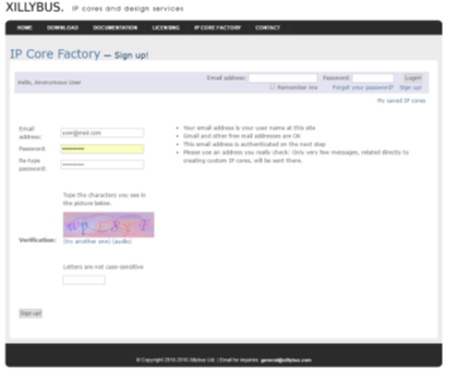
Creating new IP core
After successful registration, go to IP core Factory page [link] fill parameters as shown in Figure 39 and click Create!.
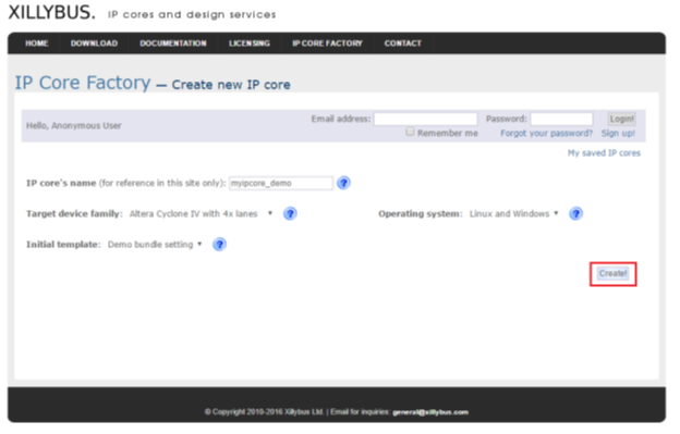
Setting core parameters
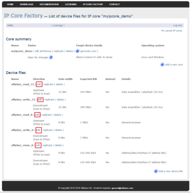
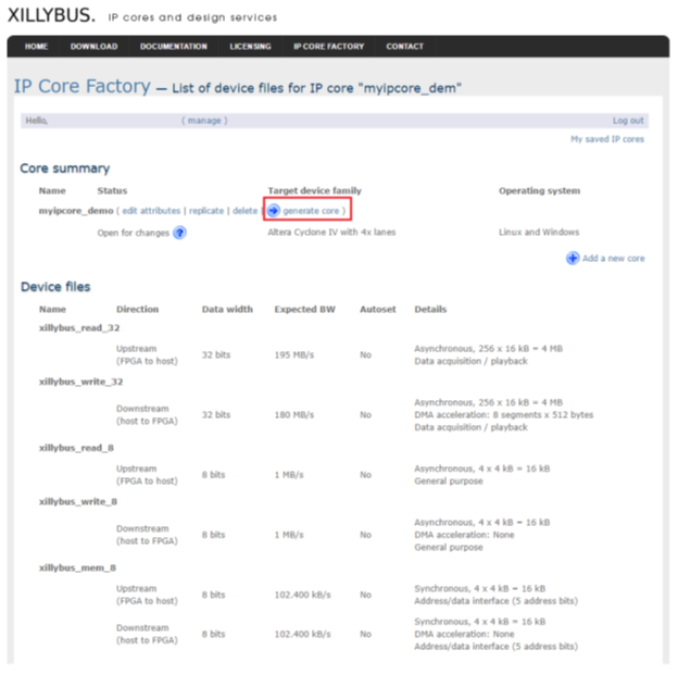
After new core creation in next dialog click Edit to change settings for each device files (Figure 40).
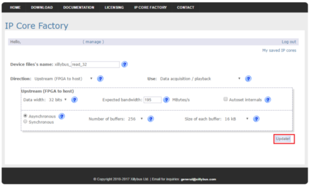
In Edit dialog (Figure 41) fill following parameters for corresponding file and click Update!. To enter all parameters Autoset internals has to be unchecked:
For xillybus_read_32:
- Device file's name - read_32
- Direction - Upstream (FPGA to host)
- Use - Data acquisition / playback
- Data width - 32 bits
- Expected bandwidth - 195
- Autoset internals - unchecked
- Asynchronous/synchronous - Asynchronous
- Number of buffers - 256
- Size of each buffer - 16 kB
Edit rest of the files with following parameters:
For xillybus_write_32:
- Device file's name - write_32
- Direction - Downstream (host to FPGA)
- Use - Data acquisition / playback
- Data width - 32 bits
- Expected bandwidth - 180
- Autoset internals - unchecked
- Asynchronous/synchronous - Asynchronous
- Number of buffers - 256
- Size of each buffer - 16 kB
- DMA acceleration - 8 segments x 512 bytes
For xillybus_read_8:
- Device file's name - read_8
- Direction - Upstream (FPGA to host)
- Use - General purpose
- Data width - 8 bits
- Expected bandwidth - 1
- Autoset internals - unchecked
- Asynchronous/synchronous - Asynchronous
- Number of buffers - 4
- Size of each buffer - 4 kB
For xillybus_write_8:
- Device file's name - write_8
- Direction - Downstream (host to FPGA)
- Use - General purpose
- Data width - 8 bits
- Expected bandwidth - 1
- Autoset internals - unchecked
- Asynchronous/synchronous - Asynchronous
- Number of buffers - 4
- Size of each buffer - 4 kB
- DMA acceleration - None
For xillybus_mem_8:
- Device file's name - mem_8
- Direction - Bidirectional
- Use - Address/data interface (5 address bits)
Upstream (FPGA to host)
- Data width - 8 bits
- Expected bandwidth - 0.1
- Autoset internals - unchecked
- Asynchronous/synchronous - Synchronous
- Number of buffers - 4
- Size of each buffer - 4kb
Downstream (host to FPGA)
- Data width - 8 bits
- Expected bandwidth - 0.1
- Autoset internals - unchecked
- Asynchronous/synchronous - Synchronous
- Number of buffers - 4
- Size of each buffer - 4kb
- DMA acceleration - None
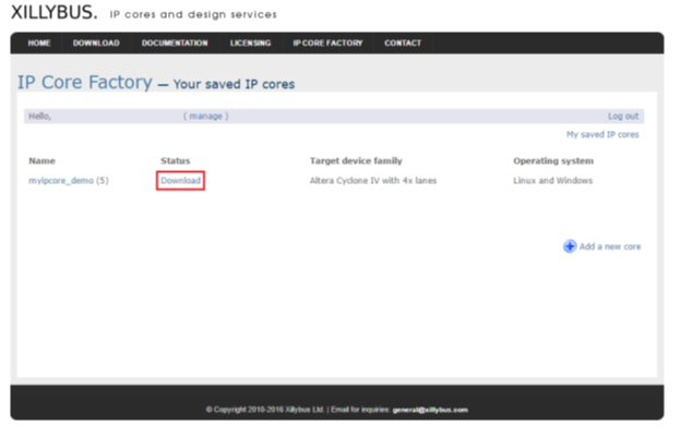
After updating all files click generate core (Figure 42). Check core status and download it when available (Figure 43).
Adding PCIe core to project
This chapter describes steps to include Xillybus core to Quartus project:
- Extract downloaded .zip file “corebundle-myipcore_demo.zip” (myipcore_demo – name that was entered during core generation).
- Place file xillybus.v to Quartus project directory limesdr-pcie_xillybus_core/
- Place file xillybus_core.qxp to Quartus project directory limesdr-pcie_xillybus_core/
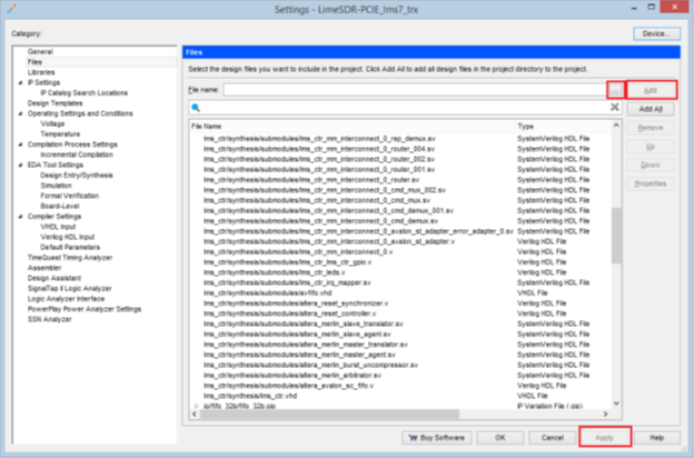
- Open Quartus LimeSDR-PCIE_lms7_trx project and select Project→ Add/Remove Files in Project.. and add files xillybus.v and xillybus_core.qxp to Quartus project (Figure 44).
- Recompile project Processing → Start Compilation.
Programming files
After performing full project compilation in Quartus prime software Processing → Start Compilation in Messages window (see Figure 45) should appear messages stating that programming files are created:

Programming files can be found in folder output_files from project directory:
- .jic - JTAG Indirect Configuration File can be used to program FPGA gateware to FLASH memory (if valid file is loaded FPGA boots from FLASH when board power is applied automatically).
- .sof - SRAM Object File can be used to program FPGA (has to be programmed every time after board power is applied)
- .rbf - Raw Binary File can be used to program FPGA gateware into FLASH memory through LimeSuiteGUI (valid gateware has to be already running, see )
Board programming procedure
For the first time use board has to be programmed using JTAG header J11. This procedure requires two computers (LimeSDR-PCIe board inserted into PCIe slot on computer #1 and Quartus Prime software running on computer #2).
- Insert LimeSDR-PCIe board into computer #1. Make sure that computer is turned off while inserting board.
- Connect one end of download cable (e.g Altera USB Blaster) to LimeSDR-PCIe board J11 connector and other end to USB port on the computer #2 running Quartus Prime software.
- Turn on computer #1 and interrupt the boot sequence to bring up the BIOS System Setup interface.
- Run Quartus Prime software in computer #2 and select Tools → Programmer
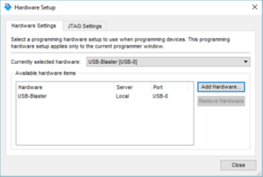
- Click Hardware Setup.. button and select your download cable, click Close (see Figure 46).
- Click Add File.. and select *.jic file (see options below):
a. Pre compiled bitstream can be found in gateware/LimeSDR-PCIE_lms7_trx_bs b. If you have followed project compilation instructions and generated your own bitstream then your file is located in project directory /output_files.
- Apply settings as in Figure 47 and click Start.
- After successful programming turn off computer #1.
- FPGA boots from programmed FLASH memory automatically when computer #1 is turned on.