LimeSDR-Mini v1.1 hardware description: Difference between revisions
Jump to navigation
Jump to search
| Line 51: | Line 51: | ||
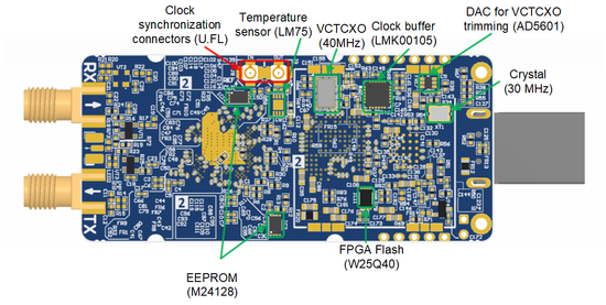
[[File:LimeSDR-Mini_v1.1_bot_componens.png|center|550px|Figure 3 LimeSDR-Mini v1.1 board bottom connectors and main componentsc ]] | [[File:LimeSDR-Mini_v1.1_bot_componens.png|center|550px|Figure 3 LimeSDR-Mini v1.1 board bottom connectors and main componentsc ]] | ||
Board components description listed in the Table 1 | Board components description listed in the Table 1. | ||
{| class="wikitable" | {| class="wikitable" | ||
| Line 84: | Line 84: | ||
|- | |- | ||
| J10 || Pin header || 5V (3.3V voltage can be chosen by resistors) fan connection pin headers, 0.1” pitch | | J10 || Pin header || 5V (3.3V voltage can be chosen by resistors) fan connection pin headers, 0.1” pitch | ||
|- | |||
! colspan="3"|Memory Devices | |||
|- | |||
| IC2 || IC || I²C EEPROM Memory 128Kb (16K x 8), connected to RF transceiver I2C bus | |||
|- | |||
| IC10 || IC || I²C EEPROM Memory 128Kb (16K x 8), connected to FPGA I2C bus | |||
|- | |||
| IC11 || IC11 || Quad SPI Flash Memory 4Mb (512K x 8), connected to FPGA SPI | |||
|- | |||
! colspan="3"|Communication Ports | |||
|- | |||
| J7 || USB3.0 connector || USB3.0 connector | |||
|- | |||
! colspan="3"|Clock Circuitry | |||
|- | |||
| XO1 || VCTCXO || 40.00 MHz Voltage Controlled Temperature Compensated Crystal Oscillatorc | |||
|- | |||
| IC9 || IC || DAC for TCXO (XT4) frequency trimming | |||
|- | |||
| IC7 || IC7 || Clock buffer | |||
|- | |||
| J8 || U.FL connector || Reference clock input | |||
|- | |||
| J9 || U.FL connector || Reference clock output | |||
|- | |||
! colspan="3"|Reference clock output | |||
|- | |||
| IC12 || IC || Switching regulator (1.8V) | |||
|- | |||
| IC13 || IC || Switching regulator (3.3V) | |||
|- | |||
| IC14 || IC || Linear regulator (2.5V) | |||
|} | |} | ||
Revision as of 08:53, 20 February 2018
LimeSDR-Mini Board Key Features
The LimeSDR-Mini is low-cost software defined radio board. LimeSDR-Mini development board provides a hardware platform for developing and prototyping high-performance and logic-intensive digital and RF designs using Intel’s MAX 10 FPGA and Lime Microsystems transceiver.

LimeSDR-Mini board features:
- USB 3.0 controller: FTDI FT601
- FPGA: Intel MAX 10 (10M16SAU169C8G 169-UBGA)
- 169-pin FBGA package
- 16 K LE
- 549 Kb M9K Memory
- 2368 Kb User Flash Memory
- 1x fractional phase locked loops (PLLs)
- 45x 18x18-bit multipliers
- 130x general purpose input/output (GPIO)
- Single supply
- Flash feature
- FPGA configuration via JTAG
- RF transceiver: Lime Microsystems LMS7002M
- EEPROM Memory: 2x 128Kb EEPROMs for LMS MCU firmware and FPGA data
- FLASH Memory: 4Mb Flash memory for FPGA data
- Temperature sensor (unpopulated)
- General user inputs/outputs:
- 1x Dual colour (RG) LED
- 8x + 2x FPGA GPIO pinheader (3.3V)
- Connections:
- USB3.0 (type A) plug
- Coaxial RF (SMA female) connectors
- FPGA GPIO headers (unpopulated)
- FPGA JTAG connector (unpopulated)
- FAN (5V or 3.3V) connector
- Clock system:
- 40.00MHz onboard VCTCXO
- Possibility to trim VCTCXO by onboard DAC
- Reference clock input and output connectors (U.FL)
- Board size: 69mm x 31.4mm
For more information on the following topics, refer to the respective documents:
- FTDI FT601 USB 3.0 to FIFO Bridge datasheet [link]
- MAX 10 FPGA device family, refer to MAX 10 Device Handbook [link]
- LMS7002M transceiver resources [link]
Board Overview
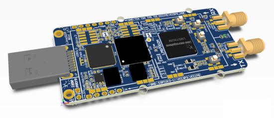
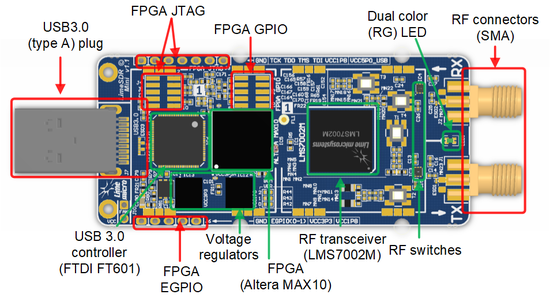
This section contains component location description on the board. LimeSDR-Mini board picture with highlighted connectors and main components is presented in Figure 2 and Figure 3.


Board components description listed in the Table 1.
| Featured Devices | ||
|---|---|---|
| Board reference | Type | Description |
| IC1 | FPRF | Field programmable RF transceiver, LMS7002M |
| IC5 | FPGA | Intel MAX 10 (10M16SAU169C8G 169-UBGA) |
| IC6 | USB 3.0 microcontroller | Intel MAX 10 (10M16SAU169C8G 169-UBGA) |
| Miscellaneous devices onboard | ||
| IC8 | IC | Temperature sensor, LM75 |
| Configuration, Status and Setup Components | ||
| J3 | JTAG chain connector | FPGA programming pin header on the board edge for Altera USB-Blaster download cable, 0.1” pitch |
| J4 | JTAG chain connector | FPGA programming pin header for Altera USB-Blaster download cable, 0.05” pitch |
| LED1 or LED2 | LED1 or LED2c | USB3.0 microcontroller (IC13) boot configuration (PMODE0[2:0]) resistors. Default mode: SPI boot, On Failure - USB Boot |
| General User Input/Output | ||
| J5 | Pin header | 8x FPGA GPIOs, 3.3V, 0.05” pitch |
| J6 | Pin header | 2x FPGA GPIOs on the board edge, 3.3V, 0.1” pitch |
| J10 | Pin header | 5V (3.3V voltage can be chosen by resistors) fan connection pin headers, 0.1” pitch |
| Memory Devices | ||
| IC2 | IC | I²C EEPROM Memory 128Kb (16K x 8), connected to RF transceiver I2C bus |
| IC10 | IC | I²C EEPROM Memory 128Kb (16K x 8), connected to FPGA I2C bus |
| IC11 | IC11 | Quad SPI Flash Memory 4Mb (512K x 8), connected to FPGA SPI |
| Communication Ports | ||
| J7 | USB3.0 connector | USB3.0 connector |
| Clock Circuitry | ||
| XO1 | VCTCXO | 40.00 MHz Voltage Controlled Temperature Compensated Crystal Oscillatorc |
| IC9 | IC | DAC for TCXO (XT4) frequency trimming |
| IC7 | IC7 | Clock buffer |
| J8 | U.FL connector | Reference clock input |
| J9 | U.FL connector | Reference clock output |
| Reference clock output | ||
| IC12 | IC | Switching regulator (1.8V) |
| IC13 | IC | Switching regulator (3.3V) |
| IC14 | IC | Linear regulator (2.5V) |