LimeSDR-QPCIe v1.2 hardware description: Difference between revisions
No edit summary |
|||
| Line 288: | Line 288: | ||
| 6 ||- ||- || | | 6 ||- ||- || | ||
|- | |- | ||
| 7 || | | 7 ||-||- || | ||
|- | |- | ||
| 8 ||- ||- || | | 8 ||- ||- || | ||
Revision as of 12:30, 18 July 2018
Introduction
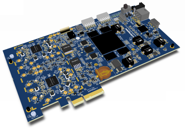
LimeSDR-QPCIe is low-cost software defined radio board based on Lime LMS7002M Field Programmable Radio Frequency (FPRF) transceiver and Altera Cyclone V PFGA, through which apps can be programmed to support any type of wireless standard, e.g. UMTS, LTE, LoRa, GPS, WiFi, Zigbee, RFID, Digital Broadcastimng, Radar and many more.
LimeSDR-QPCIe Board Key Features
The LimeSDR-QPCIe development board provides a hardware platform for developing and prototyping high-performance and logic-intensive digital and RF designs using Altera’s Cyclone V FPGA and Lime Microsystems transceiver.
For more information on the following topics, refer to the respective documents:
- Cyclone V device family, refer to Cyclone V Device support resources link
- LMS7002M transceiver resources link
LimeSDR-QPCIe v1.2 board features:
- USB Interface
- Cypress FX3 Super Speed USB 3rd generation controller
- FPGA Features
- Cyclone V, 5CGXFC7D7F31C8N device in 896-pin FBGA package
- 150’000 logic elements
- 6860 Kbits embedded memory
- 312 embedded 18x18 multipliers
- 7 PLLs
- 9 Transceivers (2.5Gbps)
- PCIe Hard IP Blocks
- 2 Hard Memory Controllers
- FPGA Configuration
- JTAG mode configuration
- Active serial mode configuration
- Possibility to update FPGA gateware by using FX3 (USB)
- Possibility to update FPGA gateware by using PCIe interface.
- RF
- 2x LMS7002M, FPRF transceivers
- Onboard RSSI measurement circuits
- Onboard loopback control switches
- DACs and ADCs
- 2x DAC5672A, dual, 14-bit, Digital-To-Analog converters
- 1x ADS424, Dual-Channel, 14-bit, Analog-To-Digital converter
- Memory Devices
- 4 x 2Gbit DDR3 SDRAM (128M x 16)
- 4Mbit flash for FX3 firmware
- 128Mbit flash for FPGA gateware
- 2 x 128Kbit and 2 x 512Kbit EEPROMs for LMS MCU firmware, LMS MCU data
- 1 x 128K EEPROM for FX3 or FPGA data
- Connections
- microUSB3.0 (type B) connector
- PCIe x4 edge connector (Gen1)
- Coaxial RF (U.FL) connectors
- 2x PMOD header (0.1” pitch)
- FPGA (0.1” pitch) and FX3 (0.05” pitch) JTAG connectors
- 12V DC power jack and pinheader
- LVDS connector (0.05” pitch)
- Fan connector (12V/5V)
- PCIe 6-pin power connector
- Holder for coin cell CR1220 battery
- Clock System
- 30.72MHz VCTCXO (precision: ±1 ppm initial, ±4 ppm stable).
- Possibility to lock VCTCXO to external clock using ADF4002 or tune VCTCXO by onboard DAC (AD5662)
- Programmable clock generator for the FPGA reference clock input or LMS PLLs
- VCTCXO clock output for external device synchronization.
- 1x 100 MHz, 4 x 125MHz crystal oscillators for FPGA
- Miscellaneous devices
- LM75 Digital temperature sensor with 2-Wire Interface.
- DS3231 real-time clock.
- M0578-A3 GPS/GNSS module receiver
- Board Size 190mm x 106.7mm (7.48” x 4.20”)
LimeSDR-QPCIe Board Overview
LimeSDR-QPCIe board version 1.2 picture with highlighted major connectors presented in Figure 2. There are three connector types – data and debugging (PCIe, USB3.0, PMOD, LVDS and JTAG), power (DC jack and external supply pinheaders) and high frequency (RF and reference clock).
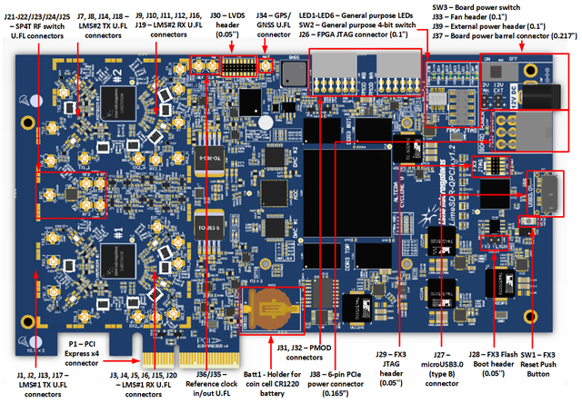
Board components description listed in the Table 1.
| Featured Devices | ||
|---|---|---|
| Board Reference | Type | Description |
| IC1, IC2 | FPRF | Field programmable RF transceivers LMS7002M |
| IC8 | FPGA | Altera Cyclone V GX, 5CGXFC7D7F31C8N, 896-BGA |
| IC13 | USB3.0 microcontroller | Cypress FX3 Supper Speed USB 3rd generation controller CYUSB3013 |
| Miscellaneous devices on board | ||
| IC7, IC8 | IC | 8-bit shift registers 74HC595BQ,115 |
| IC9, IC49 | IC | Bidirectional voltage shifters SN74AVC4T774RSVR |
| IC10, IC11, IC12, IC13, IC14, IC15, IC16, IC17 | IC | 100MHz – 3 GHz SPDT RF switches SKY13323-378LF |
| IC18, IC20, IC23, IC25, IC26, IC28 | IC | 12-bit ADCs MAX11108AVB+T |
| IC19, IC24, IC27 | IC | 1MHz–10GHz dual log detector/controller ADL5519 |
| IC22 | IC | SP4T RF switch PE42442A-Z |
| IC31 | IC | 4 parallel 2:1 switches TS3A5018PWR |
| IC37 | IC | 14-bit 2-channel ADC ADS4246IRGCT |
| IC38 | IC | Dual differential amplifier ADA4930 |
| IC39, IC56 | IC | Differential line drivers SN65LVDS1DBVR |
| IC40, IC41 | IC | Dual differential DACs DAC5672AIPFB |
| IC44, IC45 | IC | Bidirectional 8-channel voltage translators FXLA108BQX |
| IC47 | IC | Temperature sensor LM75 |
| IC48 | IC | GPS receiver module M10578-A3 |
| IC50 | IC | Real time clock (RTC) DS3231S# |
| BATT1 | Holder | Holder for coin cell CR1220 battery |
| ESD26 | TVS | USB3.0 ESD protection TVS diode |
| ESD1, ESD2, ESD3, ESD4, ESD5, ESD6, ESD7, ESD8, ESD9, ESD10, ESD11, ESD12, ESD13, ESD14, ESD15, ESD16, ESD17, ESD18, ESD19, ESD20, ESD21, ESD22, ESD23, ESD24, ESD25 | TVS | RF connector ESD protection TVS diodes |
| Configuration, Status and Setup Components | ||
| R56, R57, R58, R59 | 0 Ohm resistor | Board BOM version BOM_VER[3:0]. Default BOM_VER=0 (all resistors populated). |
| R160, R161, R163, R164, R166, R167, R168, R169, R171, R172 | 0 Ohm resistor | FPGA (IC8) MSEL[3:0]. Default mode: Active Serial Standard configuration. |
| [R268, R271, R275, R279], [R269, R273, R277, R281] | 0 Ohm resistor | DAC#1 differential channels TX1_BB_I/Q connection selection to either LMS7002M #1 or LMS7002M #2. Default populated group is [R268, R271, R275, R279]. Resistor groups are defined in [] brackets. |
| [R270, R274, R278, R282], [R272, R276, R280, R283] | 0 Ohm resistor | DAC#2 differential channels TX2_BB_I/Q connection selection to either LMS7002M #1 or LMS7002M #2. Default populated group is [R270, R274, R278, R282]. Resistor groups are defined in [] brackets. |
| R364, R379, R384 and their respective power connecting resistors R365, R380, R382 | 0 Ohm resistor | Clock buffer (IC52) CLKin0 (pin 13) clock source selection. R364 and R365 are populated by default. |
| R368, R372, R374 | 0 Ohm resistor | Clock buffer (IC52) CLKin1 (pin 28) clock source selection. R374 is populated by default. |
| R375 | 0 Ohm resistor | Clock buffer (IC52) source (CLKin0 or CLKin1) selection. If unpopulated, clock source is CLKin0 (default). If populated, clock source is CLKin1. |
| R302, R305, R307 | 10 kOhm resistor | USB3.0 microcontroller (IC13) boot configuration (PMODE0[2:0]) resistors. Default mode: SPI boot, On Failure - USB Boot |
| R294, R296, R298 | 10 kOhm resistor | USB3.0 microcontroller (IC13) crystal/clock frequency selection (FSLC[2:0]) resistors. Default mode: 19.2MHz crystal |
| J28, R313 | Pin header, 0 Ohm resistor | USB3.0 microcontroller (IC13) boot source (Flash memory or USB), 0.1” pitch jumper or 0402 0R resistor. In normal operation jumper or resistor must be placed. |
| J29 | JTAG chain pin header | USB3.0 microcontroller (IC13) debugging pin header, 0.05” pitch |
| SW1 | Push-button | USB3.0 microcontroller reset button |
| J26 | JTAG chain pin header | FPGA programming pin header for Altera USB-Blaster download cable, 0.1” pitch |
| LED1 | Green status LED | FPGA configuration done LED |
| LED2-LED5 | Green status LEDs | User defined general purpose green LEDs |
| LED6 | Red-green status LED | User defined general purpose dual colour LED |
| General User Input/Output | ||
| J31, J32 | Connector 0.1” | PMOD connectors |
| SW2 | Switch | 4-bit FPGA switch |
| J33 | Pin header | Board cooling fan pin header, 0.1” |
| Memory Devices | ||
| IC3, IC5, IC51 | EEPROM | 128Kbit (16K x 8) EEPROM, LMS7002 MCU firmware and general purpose memory |
| IC4, IC6 | EEPROM | 512Kbit (64K x 8) EEPROM, connected to main I2C bus |
| IC30 | Flash memory | 128Mbit (16M x 8) Flash for FPGA configuration (unpopulated) |
| IC32 | Flash memory | 128Mbit (16M x 8) Flash for FPGA configuration |
| IC33, IC34, IC35, IC36 | DDR3 memory | 2Gbit (128M x 16) DDR3 SDRAM |
| Communication Ports | ||
| J27 | USB3.0 connector | microUSB3.0 (type B) connector |
| P1 | PCIe connector | PCI Express (Gen1) x4 connector |
| Clock Circuitry | ||
| XO1 | VCOCXO | 10MHz voltage- and oven-controlled crystal oscillator |
| XO2, XO3 | VCTCXO | 30.72MHz voltage-controlled crystal oscillator |
| XO4 | VCTCXO | 40MHz voltage-controlled crystal oscillator |
| IC57 | IC | Programmable clock generator for the FPGA reference clock input and RF boards |
| IC53 | IC | ADF4002 phase detector |
| IC54 | IC | 16-bit DAC for VCTCXO/VCOCXO frequency tuning |
| IC52 | IC | Clock buffer |
| IC55 | IC | Clock buffer |
| J36 | U.FL connector | Reference clock input |
| J35 | U.FL connector | Reference clock output |
| XO5 | Crystal oscillator | 100MHz single-ended FPGA clock |
| XO6 | Crystal oscillator | 125MHz single-ended FPGA clock |
| XO7 | Crystal oscillator | 125MHz differential FPGA-DDR clock |
| XO8 | Crystal oscillator | 125MHz differential FPGA-DDR clock |
| XO9 | Crystal oscillator | 125MHz differential FPGA clock for PCIe REFCLK1 |
| IC56 | IC | Single-ended to differential clock converter. Clock source is IC57 pin 9. Connected to FPGA PCIe REFCLK2 and LVDS connector J30. |
| Power Supply | ||
| J37 | DC input jack | External 12V DC power supply |
| J38 | Header | 6-pin PCIe power connector, 0.165” pitch |
| J39 | Pin header | External 12V DC power supply and main internal power rail |
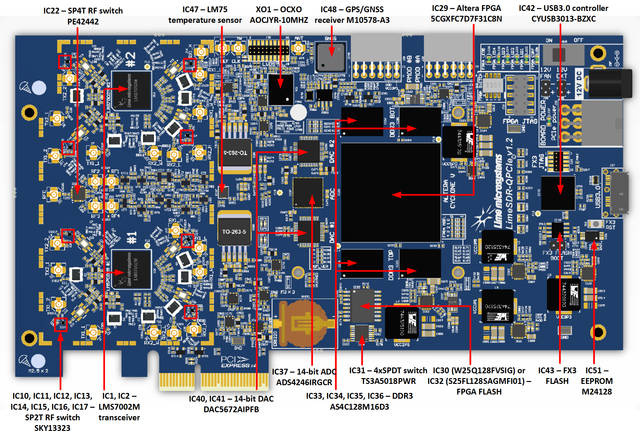
LimeSDR-QPCIe board version 1.2 picture with highlighted top components are presented in Figure 3.
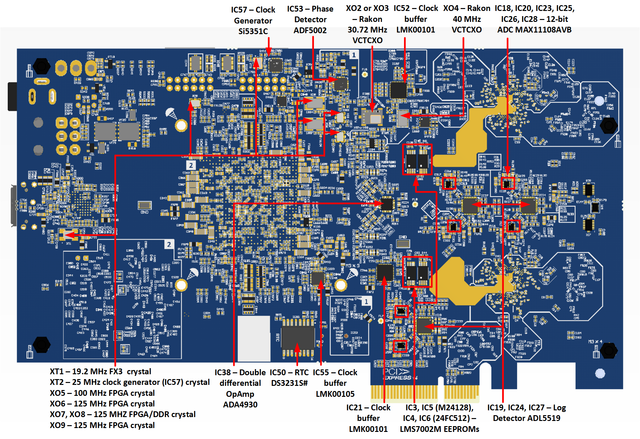
LimeSDR-QPCIe board version 1.2 picture with highlighted bottom components is presented in Figure 4.
LimeSDR-QPCIe Board Architecture
The heart of the LimeSDR-QPCIe board is Altera Cyclone V GX FPGA. Its main function is to transfer digital data between the PC through an edge PCIE and a USB3.0 connector. The block diagram for LimeSDR-QPCIe board is presented in the Figure 5.
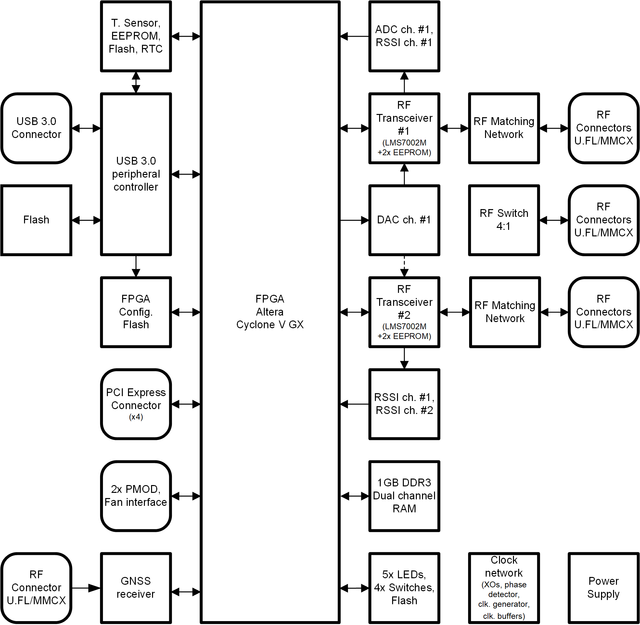
FPGA configuration
FPGA is set to use x1 Active Serial (AS) configuration scheme. In this scheme if valid configuration file exists in FLASH memory (IC30 or IC32) it is automatically loaded after power is applied to the board. In Table 2 it is listed resistor setup for Active Serial (AS) configuration mode select.
| Schematic signal name | Logic level | 0R Resistor setup | |
|---|---|---|---|
| MSEL0 | H | R160 (NF) | R161 (Fit) |
| MSEL1 | H | R163 (NF) | R164 (Fit) |
| MSEL2 | L | R166 (Fit) | R167 (NF) |
| MSEL3 | L | R168 (Fit) | R169 (NF) |
| MSEL4 | H | R171 (NF) | R172 (Fit) |
There are two options which allows to change configuration file in FLASH memory: • USB 3.0 controller – CYUSB3013 (IC42) has access to configuration memory. With valid firmware and software, gateware for FPGA can be uploaded into FLASH memory (IC30 or IC32) by using USB3.0 cable. IC42 can initiate FPGA reconfiguration. For signal interconnect details see chapter 2.2.2.3 USB 3.0 Controller. • JTAG Header – 10pin connector (J26) provides access to FPGA JTAG chain. By using external download cable such as USB-Blaster and Quartus II Programmer software FLASH memory (IC30 or IC32) can be reprogrammed. JTAG connections are listed in Table 3.
| Connector pin | Schematic signal name | FPGA pin (IC29) | Comment |
|---|---|---|---|
| 1 | FPGA_JTAG_TCK | AC7 | R170 Pull-Down resistor |
| 2 | VCC2P5 | - | |
| 3 | FPGA_JTAG_TDO | W9 | |
| 4 | VCC2P5 | - | |
| 5 | FPGA_JTAG_TMS | V7 | R162 Pull-Up resistor |
| 6 | - | - | |
| 7 | - | - | |
| 8 | - | - | |
| 9 | FPGA_JTAG_TDI | U7 | R165 Pull-Up resistor |
| 10 | GND | - |