LimeSDR-USB hardware description: Difference between revisions
No edit summary |
No edit summary |
||
| Line 178: | Line 178: | ||
The interface and control signals are described below: | The interface and control signals are described below: | ||
* Digital Interface Signals: LMS7002 is using data bus LMS_DIQ1_D[11:0] and LMS_DIQ2_D[11:0], LMS_ENABLE_IQSEL1 and LMS_ENABLE_IQSEL2, LMS_FCLK1 and LMS_FCLK2, LMS_MCLK1 and LMS_MCLK2 signals to transfer data to/from FPGA. Indexes 1 and 2 indicate transceiver digital data PORT-1 or PORT-2. Any of these ports can be used to transmit or receive data. By default, PORT-1 is selected as transmit port and PORT-2 is selected as receiver port. The FCLK# is input clock and MCLK# is output clock for LMS7002M transceiver. TXNRX signals sets ports directions. For LMS7002M interface timing details refer to LMS7002M transceiver datasheet. | * '''Digital Interface Signals''': LMS7002 is using data bus LMS_DIQ1_D[11:0] and LMS_DIQ2_D[11:0], LMS_ENABLE_IQSEL1 and LMS_ENABLE_IQSEL2, LMS_FCLK1 and LMS_FCLK2, LMS_MCLK1 and LMS_MCLK2 signals to transfer data to/from FPGA. Indexes 1 and 2 indicate transceiver digital data PORT-1 or PORT-2. Any of these ports can be used to transmit or receive data. By default, PORT-1 is selected as transmit port and PORT-2 is selected as receiver port. The FCLK# is input clock and MCLK# is output clock for LMS7002M transceiver. TXNRX signals sets ports directions. For LMS7002M interface timing details refer to LMS7002M transceiver datasheet. | ||
* '''LMS Control Signals''': these signals are used for optional functionality: | |||
** LMS_RXEN, LMS_TXEN – receiver and transmitter enable/disable signals connected to FPGA Bank 8 (VDIO_LMS_FPGA; 2.5V). | |||
** LMS_RESET – LMS7002M reset connected to FPGA Bank 7 (VDIO_LMS_FPGA; 2.5V). | |||
* '''SPI Interface''': LMS7002M transceiver is configured via 4-wire SPI interface; FPGA_SPI0_SCLK, FPGA_SPI0_MOSI, FPGA_SPI0_MISO, FPGA_SPI0_LMS_SS. The SPI interface controlled from FPGA Bank 8 (VDIO_LMS_FPGA; 2.5V). | |||
* '''Main I2C Interface''': used to control external clock synthesizer, port expander, temperature sensor, EEPROM, I2C-SPI bridge on LimeSDR-USB board. The signals FX3_I2C_SCL, FX3_I2C_SDA connected to FX3. Also these I2C lines are connected via 0R resistors to FPGA Bank 8 (VCC3P3; 3.3V) lines FPGA_I2C_SCL, FPGA_I2C_SDA. | |||
* '''LMS I2C Interface''': can be used for LMS EEPROM content modifying or for debug purposes. The signals LMS_I2C_SCL, LMS_I2C_DATA connected to FPGA Bank 8 (VDIO_LMS_FPGA; 2.5V). | |||
Revision as of 13:31, 23 August 2017
LimeSDR-USB Board Key Features
The LimeSDR-USB development board provides a hardware platform for developing and prototyping high-performance and logic-intensive digital and RF designs using Altera’s Cyclone IV FPGA and Lime Microsystems transceiver.
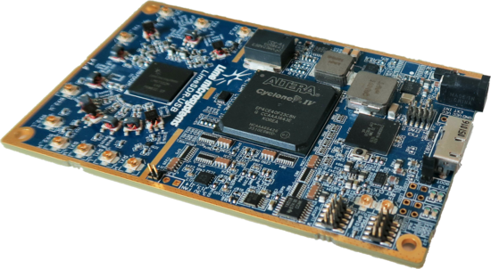
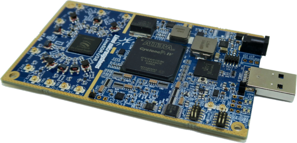
The LimeSDR-USB has two different USB connector versions. LimeSDR-USB 1v4 is micro USB type B connector (socket) based, as shown in Figure 1. LimeSDR-USB 1v4s is a USB type A connector (plug) based, as shown in Figure 2.
LimeSDR-USB board features:
- USB Interface
- Cypress FX3 Super Speed USB 3rd generation controller
- FPGA Features
- Cyclone IV EP4CE40F23C8N device in 484-pin FPGA
- 39’600 logic elements
- 1134 Kbits embedded memory
- 116 embedded 18x18 multipliers
- 4 PLLs
- FPGA Configuration
- JTAG mode configuration
- Active serial mode configuration
- Possibility to update FPGA gateware by using FX3 (USB)
- Memory Devices
- 2x 1Gbit (64M x 16) DDR2 SDRAM
- 4Mbit flash for FX3 firmware
- 16Mbit flash for FPGA gateware
- 2 x 128K (16K x 8) EEPROMs for LMS MCU firmware, LMS MCU data
- 1 x 64K (8K x 8) EEPROM for FX3 data
- Connections
- microUSB3.0 (type B) connector or USB3.0 (type A) plug
- Coaxial RF (U.FL) connectors
- FPGA GPIO headers (0.05” pitch)
- FPGA and FX3 JTAG connectors (0.05” pitch)
- 6..12V DC power jack and pinheader
- Fan connector (3.3V)
- Clock System
- 30.72MHz VCTCXO (precision: ±1 ppm initial, ±4 ppm stable).
- Possibility to lock VCTCXO to external clock or tune VCTCXO by onboard DAC
- Programmable clock generator for the FPGA reference clock input or LMS PLLs
- Board Size 60mm x 100mm (2.36” x 3.94”)
LimeSDR-USB board overview
LimeSDR-USB board version 1.4 picture with highlighted major connections presented in Figure 3. There are three connector types – data and debugging (USB3.0, FPGA GPIO and JTAG), power (DC jack and external supply pinheader) and high frequency (RF and reference clock).
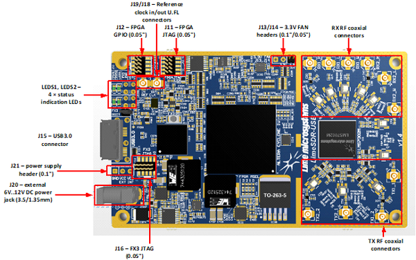
Board components description listed in the Table 1 and Table 2.
| Featured Devices | ||
|---|---|---|
| Board reference | Type | Description |
| IC1 | FPRF | Field programmable RF transceiver, LMS7002M |
| IC8 | FPGA | Altera Cyclone IV, EP4CE40F23C8N 484-BGA |
| IC13 | USB 3.0 microcontroller | Cypress FX3 Super Speed USB 3rd generation controller, CYUSB3014 |
| Miscellaneous devices onboard | ||
| IC9 | IC | Quad SPDT switch, TS3A5018PW |
| IC6 | IC | Temperature sensor, LM75 |
| IC19 | IC | SPI to I²C bridge, SC18IS602BIPW (not mounted) |
| IC17 | IC | I²C port expander with 4 push-pull outputs and 4 inputs, MAX7322ATE+ |
| Configuration, Status and Setup Components | ||
| IC9 | IC | Quad SPDT switch, TS3A5018PW |
| R51, R52, R53, R54, R56, R57, R59, R60 | 0 Ohm resistor | FPGA (IC31) MSEL[3:0]. Default mode: Active Serial Standard configuration |
| R115, R116, R117 | 10 kOhm resistor | USB3.0 microcontroller (IC13) boot configuration (PMODE0[2:0]) resistors. Default mode: SPI boot, On Failure - USB Boot |
| R125, R127, R128 | 10 kOhm resistor | USB3.0 microcontroller (IC13) crystal/clock frequency selection (FSLC[2:0]) resistors. Default mode: 19.2MHz crystal |
| J16 | JTAG chain pin header | USB3.0 (IC6) microcontroller’s debugging pin header, 0.05” pitch |
| J17, R122 | Pin header | USB3.0 microcontroller boot source (Flash memory or USB), 0.05” pitch jumper or 0402 0R resistor. In normal operation jumper or resistor must be placed. |
| SW1 | Push-button | USB3.0 microcontroller reset button |
| J11 | JTAG chain pin header | FPGA programming pin header for Altera USB-Blaster download cable, 0.05” pitch |
| LEDS1 | Red-green status LEDs | User defined FPGA indication LED1 (near board edge if SMD; on the bottom if through-hole), User defined FPGA indication LED2 (farther board edge if SMD; on the top if through-hole) |
| LEDS2 | Red-green status LEDs | FX3 (USB) status indication LED (near board edge if SMD; on the bottom if through-hole), board power indication LED (farther board edge if SMD; on the top if through-hole) |
| General User Input/Output | ||
| J12 | Pin header | 8 FPGA GPIOs, 0.05” pitch |
| J13, J14 | Pin header | 3.3V fan connection pin headers, 0.1” and 0.05” pitch respectively |
| Memory Devices | ||
|---|---|---|
| Board reference | Type | Description |
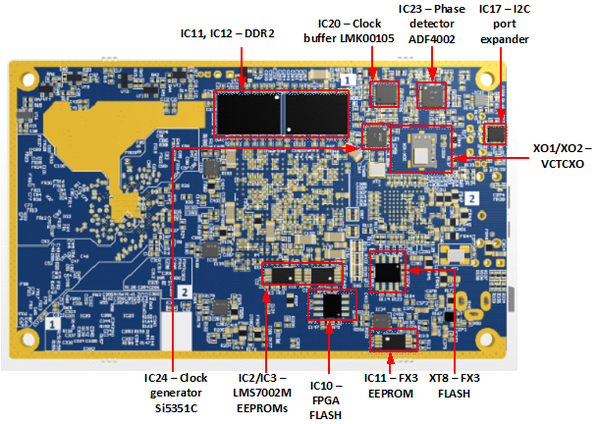
| IC11, IC12 | DDR2 memory | 1Gbit (64M x 16) DDR2 SDRAM with a 16-bit data bus |
| IC2, IC3 | EEPROM | 128K (16K x 8) EEPROM, LMS7002 MCU firmware, LMS7002M data |
| IC18 | EEPROM | 64K (8K x 8) EEPROM, connected to main I2C bus |
| IC10 | Flash memory | 16Mbit Flash for FPGA configuration |
| IC15 | Flash memory | 4Mbit Flash for FX3 firmware |
| Communication Ports | ||
| J15 | USB3.0 connector | microUSB3.0 (type B) connector or USB3.0 (type A) plug |
| Clock Circuitry | ||
| XO1, XO2 | VCTCXO | 30.72MHz voltage-controlled crystal oscillator |
| IC24 | IC | Programmable clock generator for the FPGA reference clock input and RF boards |
| IC23 | IC | ADF4002 phase detector |
| IC22 | IC | DAC for TCXO (XT4) frequency tuning |
| J19 | U.FL connector | Reference clock input |
| J18 | U.FL connector | Reference clock output |
| Power Supply | ||
| J20 | DC input jack | External 6V..12V DC power supply |
| J21 | Pin header | External 6V..12V DC power supply and main internal power rail |
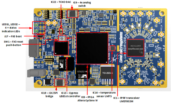
LimeSDR-USB board version 1.4 picture with highlighted top components are presented in Figure 4.
LimeSDR-USB board version 1.4 picture with highlighted bottom components is presented in Figure 5.
LimeSDR-USB board architecture
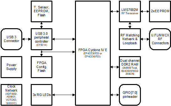
The heart of the LimeSDR-USB board is Altera Cyclone IV FPGA. Its main function is to transfer digital data between the PC through a USB3.0 connector. The block diagram for LimeSDR-USB board is presented in the Figure 6.
LMS7002M based connectivity
The interface and control signals are described below:
- Digital Interface Signals: LMS7002 is using data bus LMS_DIQ1_D[11:0] and LMS_DIQ2_D[11:0], LMS_ENABLE_IQSEL1 and LMS_ENABLE_IQSEL2, LMS_FCLK1 and LMS_FCLK2, LMS_MCLK1 and LMS_MCLK2 signals to transfer data to/from FPGA. Indexes 1 and 2 indicate transceiver digital data PORT-1 or PORT-2. Any of these ports can be used to transmit or receive data. By default, PORT-1 is selected as transmit port and PORT-2 is selected as receiver port. The FCLK# is input clock and MCLK# is output clock for LMS7002M transceiver. TXNRX signals sets ports directions. For LMS7002M interface timing details refer to LMS7002M transceiver datasheet.
- LMS Control Signals: these signals are used for optional functionality:
- LMS_RXEN, LMS_TXEN – receiver and transmitter enable/disable signals connected to FPGA Bank 8 (VDIO_LMS_FPGA; 2.5V).
- LMS_RESET – LMS7002M reset connected to FPGA Bank 7 (VDIO_LMS_FPGA; 2.5V).
- SPI Interface: LMS7002M transceiver is configured via 4-wire SPI interface; FPGA_SPI0_SCLK, FPGA_SPI0_MOSI, FPGA_SPI0_MISO, FPGA_SPI0_LMS_SS. The SPI interface controlled from FPGA Bank 8 (VDIO_LMS_FPGA; 2.5V).
- Main I2C Interface: used to control external clock synthesizer, port expander, temperature sensor, EEPROM, I2C-SPI bridge on LimeSDR-USB board. The signals FX3_I2C_SCL, FX3_I2C_SDA connected to FX3. Also these I2C lines are connected via 0R resistors to FPGA Bank 8 (VCC3P3; 3.3V) lines FPGA_I2C_SCL, FPGA_I2C_SDA.
- LMS I2C Interface: can be used for LMS EEPROM content modifying or for debug purposes. The signals LMS_I2C_SCL, LMS_I2C_DATA connected to FPGA Bank 8 (VDIO_LMS_FPGA; 2.5V).