LimeSDR-QPCIe Board Programming: Difference between revisions
| (14 intermediate revisions by the same user not shown) | |||
| Line 2: | Line 2: | ||
This document describes how to program LimeSDR-QPCie board using LimeSuiteGUI and Cypress (for FX3 MCU only) software. | This document describes how to program LimeSDR-QPCie board using LimeSuiteGUI and Cypress (for FX3 MCU only) software. | ||
== Updating FX3 Firmware using LimeSuiteGUI == | |||
The firmware of FX3 MCU contains a functionality which enables to program FLASH memory FX3 MCU boots up from. In this case FX3 USB controller firmware can be updated using “LimeSuiteGUI” software, when FX3 MCU can boot from FLASH memory. | |||
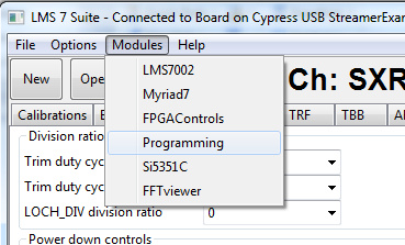
To call FPGA programing function, launch LimeSuiteGUI and connect to the board (see [[Getting_Started_with_LimeSDR-USB_and_LimeSuiteGUI#Launching_LimeSuiteGUI_and_Connecting_to_the_Board | Launching LimeSuiteGUI and Connecting to the Board]] for more information). Then go to Modules from main menu and select Programing form the drop down menu, as shown in Figure 1. | |||
[[File:LimeSDR-USB-LMS-7-Suite-Modules-Programming.jpg|thumb|center|600px|Figure 1. LimeSuiteGUI module menu to select FX3 programing tool]] | |||
New window appears, as shown in the Figure 2. | |||
[[File:LimeSDR-USB-LMS-7-Suite-Modules-Programming-Section.jpg|thumb|center|600px|Figure 2. Programing tool interface]] | |||
Change device to “FX3” and press “Open” and select firmware image file. | |||
[[File:FX3_programing_options.png|thumb|center|600px|Figure 3. FX3 programing options]] | |||
Initiate FLASH memory programing by clicking Program. | |||
The new message will come up when programing is finished, as shown in Figure 4. | |||
[[File:Successfully_FX3_programing_message.png|thumb|center|600px|Figure 4. Successfully FX3 programing message ]] | |||
After successful firmware update, connect to the LimeSDR-QPCIe board again as described in [[Getting_Started_with_LimeSDR-USB_and_LimeSuiteGUI#Launching_LimeSuiteGUI_and_Connecting_to_the_Board | Launching LimeSuiteGUI and Connecting to the Board]]. | |||
== Updating USB3 Microcontroller Firmware in Bootloader Mode == | == Updating USB3 Microcontroller Firmware in Bootloader Mode == | ||
| Line 9: | Line 37: | ||
For USB microcontroller firmware upgrade, please use the “CyControl.exe” application from cy_ssusbsuite_v1.3.3.zip package. | For USB microcontroller firmware upgrade, please use the “CyControl.exe” application from cy_ssusbsuite_v1.3.3.zip package. | ||
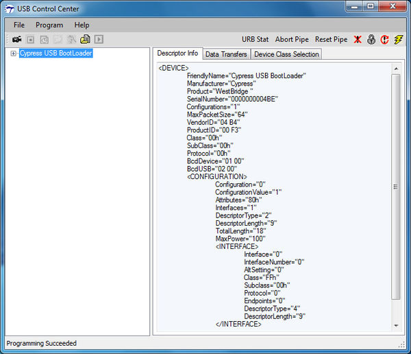
If FLASH memory is empty or connector | If FLASH memory is empty or connector J28 (on LimeSDR-QPCIe board) is open, USB3 microcontroller boots-up into bootloader mode. Cypress drivers from cy_ssusbsuite_v1.3.3.zip package must be installed first. Download the package [https://www.cypress.com/documentation/software-and-drivers/ez-usb-fx3-software-development-kit here]. Run the “USB Control Center” application and select Cypress USB BootLoader line as shown in Figure 5. | ||
[[File:LimeSDR-USB-Control-Center.jpg|thumb|center|600px|Figure 5. Default FX3 firmware, supplied by FX3 internal logic]] | [[File:LimeSDR-USB-Control-Center.jpg|thumb|center|600px|Figure 5. Default FX3 firmware, supplied by FX3 internal logic]] | ||
| Line 22: | Line 50: | ||
=== Uploading Firmware to SPI FLASH Memory === | === Uploading Firmware to SPI FLASH Memory === | ||
Short the jumper | Short the jumper J28 and connect LimeSDR-QPCIe board to the PC. Start “CyControl.exe” application and select Cypress USB BootLoader as shown in Figure 5. Choose menu command Program -> FX3 -> SPI FLASH. In the status bar you will see Waiting for Cypress Boot Programmer device to enumerate.... and after some time window will appear. Select firmware image file (file extension is “*.img”) and press Open. Status bar of the USB Control Center application will indicate Programming of SPI FLASH in Progress…. This message will change to the Programming succeeded after FLASH programming is done. | ||
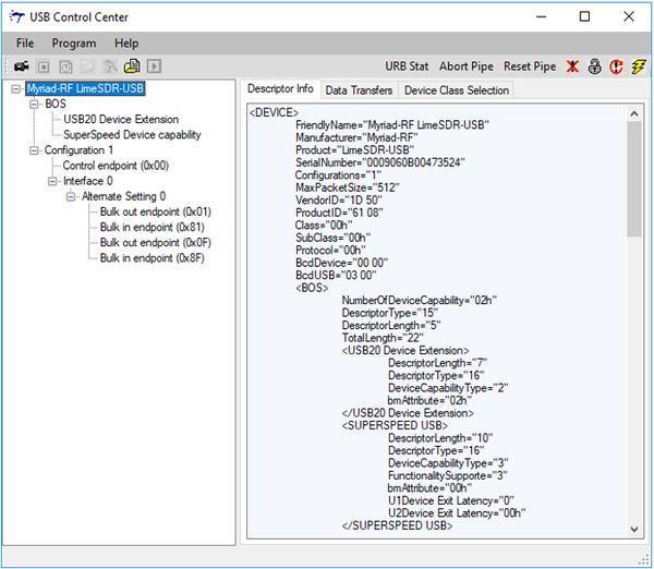
If you expand Cypress USB StreamerExample line in USB Control Center application now, you will see different USB configuration as shown in Figure 6. | If you expand Cypress USB StreamerExample line in USB Control Center application now, you will see different USB configuration as shown in Figure 6. | ||
| Line 29: | Line 57: | ||
NOTE: USB3 microcontroller will boot firmware uploaded to FLASH each time after power-on if jumper | NOTE: USB3 microcontroller will boot firmware uploaded to FLASH each time after power-on if jumper J28 is shorted. | ||
=== Uploading Firmware to the FX3 RAM === | === Uploading Firmware to the FX3 RAM === | ||
| Line 35: | Line 63: | ||
Start “CyControl.exe” application and select Cypress USB BootLoader as shown in Figure 5. Choose menu command Program -> FX3 -> RAM. In the new pop-up window, select firmware image file (file extension is “*.img”) and press Open. Status bar of the USB Control Center application will indicate Programming RAM. This message will change to the Programming succeeded after programming is done. | Start “CyControl.exe” application and select Cypress USB BootLoader as shown in Figure 5. Choose menu command Program -> FX3 -> RAM. In the new pop-up window, select firmware image file (file extension is “*.img”) and press Open. Status bar of the USB Control Center application will indicate Programming RAM. This message will change to the Programming succeeded after programming is done. | ||
Note please that this may be used for test purposes only, while firmware will disappear from the RAM after LimeSDR- | Note please that this may be used for test purposes only, while firmware will disappear from the RAM after LimeSDR-QPCIe board power cycle. | ||
== | === Uploading FPGA Gateware to FLASH Memory === | ||
There are two ways of uploading FPGA gateware to onboard FLASH memory: | |||
* Using LimeSuiteGUI (requires FX3 Firmware to be already uploaded) | |||
* Using JTAG programming cable | |||
==== Uploading FPGA Gateware to FLASH Memory using LimeSuiteGUI ==== | |||
This section describes how to load custom gateware to LimeSDR-QPCIe board FPGA Flash memory. | |||
The Altera Cyclone V FPGA which sits on the LimeSDR-QPCIe board can be programmed using “LimeSuiteGUI”software. To call FPGA programing function, go to Modules from main menu and select Programing form the drop down menu, as shown in Figure 1. | |||
New window appears, as shown in the Figure 2. | New window appears, as shown in the Figure 2. | ||
[[File:LimeSDR-USB-LMS-7-Suite-Modules-Programming- | Software loads raw programming data files (*.rpd) to FPGA and it offers couple options to do that, see Figure 7. | ||
[[File:LimeSDR-USB-LMS-7-Suite-Modules-Programming-Mode.jpg|thumb|center|600px|Figure 7. FPGA programing options]] | |||
Select Bitstream to FLASH programming mode. This function loads selected *.rpd file from PC to external FPGA FLASH memory. Select required bitstream file by clicking Open and initiate FLASH memory programing by clicking on Program. | |||
The new message will come up when the programing is finished, as shown in Figure 8. | |||
[[File:LimeSDR-USB-LMS-7-Suite-Modules-Programming-Complete.jpg|thumb|center|600px|Figure 8. FPGA programmed successfully]] | |||
After writing new bitstream to Flash memory, it can be loaded to FPGA by changing Programing mode to Bitstream from Flash and pressing Program. New bitstream will be loaded to FPGA. Each time board is powered up, FPGA bitstream is loaded from FLASH automatically. | |||
==== Uploading FPGA gateware to FLASH memory using JTAG Cable ==== | |||
For the first time use board can be programmed using JTAG header J26. This procedure requires two computers (LimeSDR-QPCIe board inserted into PCIe slot on computer #1 and Quartus Prime software running on computer #2). | |||
* Insert LimeSDR-QPCIe board into computer #1. Make sure that computer is turned off while inserting board. | |||
* Connect one end of download cable (e.g Altera USB Blaster) to LimeSDR-QPCIe board J26 connector and other end to USB port on the computer #2 running Quartus Prime software. | |||
* Turn on computer #1 and interrupt the boot sequence to bring up the BIOS System Setup interface. | |||
* Run Quartus Prime software in computer #2 and select Tools → Programmer | |||
* Click Hardware Setup.. button and select your download cable, click Close (see Figure 9). | |||
[[File:LimeSDR-QPCIe-JTAG_Selecting programming hardware.png|thumb|center|600px|Figure 9 Selecting programming hardware]] | |||
* Click Add File.. and select *.jic file (see options below): | |||
<ol style="list-style-type:lower-alpha"> | |||
<li>Pre compiled bitstream can be found in gateware/LimeSDR-QPCIE_lms7_trx_bs</li> | |||
<li> If you have followed project compilation instructions and generated your own bitstream then your file is located in project directory /output_files.</li> | |||
</ol> | |||
* Apply settings as in Figure 10 and click Start. | |||
[[File:LimeSDR-QPCIe-JTAG_Adding_programming_file.png|thumb|center|600px|Figure 10 Adding programming file]] | |||
* After successful programming turn off computer #1. | |||
* FPGA boots from programmed FLASH memory automatically when computer #1 is turned on. | |||
=== Obtaining FPGA programming files === | |||
FPGA gateware programming file can be obtained by compiling provided LimeSDR-QPCIE_lms7_trx project with Intel Quartus Prime software. Software version used with this guide: Quartus prime 15.1.2 Build 193 02/01/2016 SJ Lite Edition. Quartus Prime Lite Edition software can be downloaded from [http://dl.altera.com/15.1/?edition=lite&platform=windows&download_manager=dlm3 here]. | |||
==== PCIe core generation ==== | |||
PCIe Xillybus core has to be generated and downloaded in order to compile LimeSDR-QPCIE_lms7_trx FPGA project. This chapter describes steps and parameters required to generate Xillybus PCIe core. | |||
==== Signing UP ==== | |||
Xillybus requires to fill up free registration form in order to download generated core. Go to [http://xillybus.com/ipfactory/signup link], fill required fields (Figure 11) and confirm registration via received eMail. | |||
[[File:LimeSDR-QPCIe-COREGEN_Registration form.png|thumb|center|600px|Figure 11 Registration form]] | |||
==== Creating new IP core ==== | |||
After successful registration, go to IP core Factory page [http://xillybus.com/ipfactory/ link] fill parameters as shown in Figure 12 and click Create!. | |||
[[File:LimeSDR-QPCIe-COREGEN_Create new IP core dialog.png|thumb|center|600px|Figure 12 Create new IP core dialog]] | |||
==== Setting core parameters ==== | |||
After new core creation in next dialog click Edit to change settings for each device files (Figure 13). | |||
[[File:LimeSDR-QPCIe-COREGEN_File editing.png|thumb|center|600px|Figure 13 File editing]] | |||
In Edit dialog (Figure 14) fill following parameters for corresponding file and click Update!. To enter all parameters Autoset internals has to be unchecked: | |||
<nowiki>For xillybus_read_32: | |||
• Device file's name - stream0_read_32 | |||
• Direction - Upstream (FPGA to host) | |||
• Use - Data acquisition / playback | |||
• Data width - 32 bits | |||
• Expected bandwidth - 395 | |||
• Autoset internals - unchecked | |||
• Asynchronous/synchronous - Asynchronous | |||
• Number of buffers - 512 | |||
• Size of each buffer - 16 kB </nowiki> | |||
[[File:LimeSDR-QPCIe-COREGEN_xillybus_read_32 file editing.png|thumb|center|600px|Figure 14 File editing]] | |||
Edit rest of the files with following parameters: | |||
<nowiki>For xillybus_write_32: | |||
• Device file's name - stream0_write_32 | |||
• Direction - Downstream (host to FPGA) | |||
• Use - Data acquisition / playback | |||
• Data width - 32 bits | |||
• Expected bandwidth - 395 | |||
• Autoset internals - unchecked | |||
• Asynchronous/synchronous - Asynchronous | |||
• Number of buffers - 512 | |||
• Size of each buffer - 16 kB | |||
• DMA acceleration - 8 segments x 512 bytes | |||
For xillybus_read_8: | |||
• Device file's name - control0_read_32 | |||
• Direction - Upstream (FPGA to host) | |||
• Use - General purpose | |||
• Data width - 32 bits | |||
• Expected bandwidth - 1 | |||
• Autoset internals - checked | |||
For xillybus_write_8: | |||
• Device file's name - control0_write_32 | |||
• Direction - Downstream (host to FPGA) | |||
• Use - General purpose | |||
• Data width - 32 bits | |||
• Expected bandwidth - 1 | |||
• Autoset internals - checked | |||
For xillybus_mem_8: | |||
• Device file's name - mem_8 | |||
• Direction - Bidirectional | |||
• Use - Address/data interface (5 address bits) | |||
Upstream (FPGA to host) | |||
o Data width - 8 bits | |||
o Expected bandwidth - 0.1 | |||
o Autoset internals - checked | |||
Downstream (host to FPGA) | |||
o Data width - 8 bits | |||
o Expected bandwidth - 0.1 | |||
o Autoset internals - checked</nowiki> | |||
Next step is to add more device files, click Add new device file Figure 15 and add following device files with following parameters: | |||
<nowiki>xillybus_stream1_read_32: | |||
• Device file's name - stream1_read_32 | |||
• Direction - Upstream (FPGA to host) | |||
• Use - Data acquisition / playback | |||
• Data width - 32 bits | |||
• Expected bandwidth - 395 | |||
• Autoset internals - unchecked | |||
• Asynchronous/synchronous - Asynchronous | |||
• Number of buffers - 512 | |||
• Size of each buffer - 16 kB | |||
xillybus_ stream1_write_32: | |||
• Device file's name - stream1_write_32 | |||
• Direction - Downstream (host to FPGA) | |||
• Use - Data acquisition / playback | |||
• Data width - 32 bits | |||
• Expected bandwidth - 395 | |||
• Autoset internals - unchecked | |||
• Asynchronous/synchronous - Asynchronous | |||
• Number of buffers - 512 | |||
• Size of each buffer - 16 kB | |||
• DMA acceleration - 8 segments x 512 bytes | |||
xillybus_stream2_read_32: | |||
• Device file's name - stream2_read_32 | |||
• Direction - Upstream (FPGA to host) | |||
• Use - Data acquisition / playback | |||
• Data width - 32 bits | |||
• Expected bandwidth - 395 | |||
• Autoset internals - unchecked | |||
• Asynchronous/synchronous - Asynchronous | |||
• Number of buffers - 512 | |||
• Size of each buffer - 16 kB | |||
xillybus_stream2_write_32: | |||
• Device file's name - stream2_write_32 | |||
• Direction - Downstream (host to FPGA) | |||
• Use - Data acquisition / playback | |||
• Data width - 32 bits | |||
• Expected bandwidth - 395 | |||
• Autoset internals - unchecked | |||
• Asynchronous/synchronous - Asynchronous | |||
• Number of buffers - 512 | |||
• Size of each buffer - 16 kB | |||
• DMA acceleration - 8 segments x 512 bytes | |||
</nowiki> | |||
[[File:LimeSDR-QPCIe-COREGEN_Add new device file .png|thumb|center|600px|Figure 15 Add new device file ]] | |||
After updating all files click generate core (Figure 16). Check core status and download it when available (Figure 17). | |||
[[File:LimeSDR-QPCIe-COREGEN_Core generation.png|thumb|center|600px|Figure 16 Core generation]] | |||
[[File:LimeSDR-QPCIe-COREGEN_Download status .png|thumb|center|600px|Figure 17 Download status]] | |||
==== Adding PCIe core to project ==== | |||
This chapter describes steps to include Xillybus core to Quartus project: | |||
* Extract downloaded .zip file “corebundle-myipcore_demo.zip” (myipcore_demo – name that was entered during core generation). | |||
* Place file xillybus.v to Quartus project directory limesdr-qpcie_xillybus_core/ | |||
* Place file xillybus_core.qxp to Quartus project directory limesdr-qpcie_xillybus_core/ | |||
* Open Quartus LimeSDR-QPCIE_lms7_trx project and select Project→ Add/Remove Files in Project.. and add files xillybus.v and xillybus_core.qxp to Quartus project (Figure 82). | |||
* Recompile project Processing → Start Compilation. | |||
[[File:LimeSDR-QPCIe-COREGEN_Adding files to Quartus project .png|thumb|center|600px|Figure 18 Adding files to Quartus project]] | |||
==== Programming files ==== | |||
After performing full project compilation in Quartus prime software Processing → Start Compilation in Messages window (see Figure 19) should appear messages stating that programming files are created: | |||
[[File:LimeSDR-QPCIe-COREGEN_Project compilation message window.png|thumb|center|600px|Figure 19 Project compilation message window]] | |||
Programming files can be found in folder output_files from project directory: | |||
*.jic - JTAG Indirect Configuration File can be used to program FPGA gateware to FLASH memory (if valid file is loaded FPGA boots from FLASH when board power is applied automatically). | |||
*.sof - SRAM Object File can be used to program FPGA (has to be programmed every time after board power is applied) | |||
*.rbf - Raw Binary File can be used to program FPGA gateware into FLASH memory through LimeSuiteGUI (valid gateware has to be already running) | |||
Latest revision as of 16:13, 12 March 2019
LimeSDR-QPCIe Board Programming
This document describes how to program LimeSDR-QPCie board using LimeSuiteGUI and Cypress (for FX3 MCU only) software.
Updating FX3 Firmware using LimeSuiteGUI
The firmware of FX3 MCU contains a functionality which enables to program FLASH memory FX3 MCU boots up from. In this case FX3 USB controller firmware can be updated using “LimeSuiteGUI” software, when FX3 MCU can boot from FLASH memory.
To call FPGA programing function, launch LimeSuiteGUI and connect to the board (see Launching LimeSuiteGUI and Connecting to the Board for more information). Then go to Modules from main menu and select Programing form the drop down menu, as shown in Figure 1.
New window appears, as shown in the Figure 2.

Change device to “FX3” and press “Open” and select firmware image file.

Initiate FLASH memory programing by clicking Program.
The new message will come up when programing is finished, as shown in Figure 4.

After successful firmware update, connect to the LimeSDR-QPCIe board again as described in Launching LimeSuiteGUI and Connecting to the Board.
Updating USB3 Microcontroller Firmware in Bootloader Mode
Cypress FX3 USB microcontroller has an integrated boot loader, which starts automatically after power-up or reset and when no valid firmware is present in the FLASH memory.
For USB microcontroller firmware upgrade, please use the “CyControl.exe” application from cy_ssusbsuite_v1.3.3.zip package.
If FLASH memory is empty or connector J28 (on LimeSDR-QPCIe board) is open, USB3 microcontroller boots-up into bootloader mode. Cypress drivers from cy_ssusbsuite_v1.3.3.zip package must be installed first. Download the package here. Run the “USB Control Center” application and select Cypress USB BootLoader line as shown in Figure 5.
After entering into boot loader mode, there are two ways of uploading the firmware to USB3 microcontroller:
- Program external SPI FLASH memory connected to USB3 controller. Follow procedure described in chapter “5.3 Uploading Firmware to SPI FLASH”. The USB3 microcontroller will boot from FLASH memory after every power-on.
- Program internal RAM memory. Follow procedure described in chapter “5.4 Uploading Firmware to the FX3 RAM”. The memory will be cleared after first power cycle hence this step should be used for test purposes only.
Uploading Firmware to SPI FLASH Memory
Short the jumper J28 and connect LimeSDR-QPCIe board to the PC. Start “CyControl.exe” application and select Cypress USB BootLoader as shown in Figure 5. Choose menu command Program -> FX3 -> SPI FLASH. In the status bar you will see Waiting for Cypress Boot Programmer device to enumerate.... and after some time window will appear. Select firmware image file (file extension is “*.img”) and press Open. Status bar of the USB Control Center application will indicate Programming of SPI FLASH in Progress…. This message will change to the Programming succeeded after FLASH programming is done.
If you expand Cypress USB StreamerExample line in USB Control Center application now, you will see different USB configuration as shown in Figure 6.
NOTE: USB3 microcontroller will boot firmware uploaded to FLASH each time after power-on if jumper J28 is shorted.
Uploading Firmware to the FX3 RAM
Start “CyControl.exe” application and select Cypress USB BootLoader as shown in Figure 5. Choose menu command Program -> FX3 -> RAM. In the new pop-up window, select firmware image file (file extension is “*.img”) and press Open. Status bar of the USB Control Center application will indicate Programming RAM. This message will change to the Programming succeeded after programming is done.
Note please that this may be used for test purposes only, while firmware will disappear from the RAM after LimeSDR-QPCIe board power cycle.
Uploading FPGA Gateware to FLASH Memory
There are two ways of uploading FPGA gateware to onboard FLASH memory:
- Using LimeSuiteGUI (requires FX3 Firmware to be already uploaded)
- Using JTAG programming cable
Uploading FPGA Gateware to FLASH Memory using LimeSuiteGUI
This section describes how to load custom gateware to LimeSDR-QPCIe board FPGA Flash memory.
The Altera Cyclone V FPGA which sits on the LimeSDR-QPCIe board can be programmed using “LimeSuiteGUI”software. To call FPGA programing function, go to Modules from main menu and select Programing form the drop down menu, as shown in Figure 1.
New window appears, as shown in the Figure 2.
Software loads raw programming data files (*.rpd) to FPGA and it offers couple options to do that, see Figure 7.
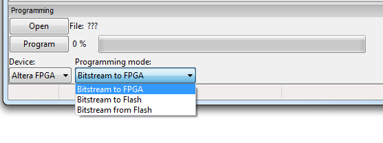
Select Bitstream to FLASH programming mode. This function loads selected *.rpd file from PC to external FPGA FLASH memory. Select required bitstream file by clicking Open and initiate FLASH memory programing by clicking on Program.
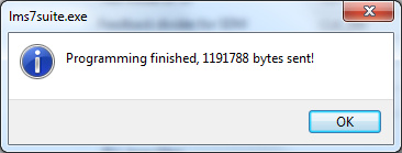
The new message will come up when the programing is finished, as shown in Figure 8.
After writing new bitstream to Flash memory, it can be loaded to FPGA by changing Programing mode to Bitstream from Flash and pressing Program. New bitstream will be loaded to FPGA. Each time board is powered up, FPGA bitstream is loaded from FLASH automatically.
Uploading FPGA gateware to FLASH memory using JTAG Cable
For the first time use board can be programmed using JTAG header J26. This procedure requires two computers (LimeSDR-QPCIe board inserted into PCIe slot on computer #1 and Quartus Prime software running on computer #2).
- Insert LimeSDR-QPCIe board into computer #1. Make sure that computer is turned off while inserting board.
- Connect one end of download cable (e.g Altera USB Blaster) to LimeSDR-QPCIe board J26 connector and other end to USB port on the computer #2 running Quartus Prime software.
- Turn on computer #1 and interrupt the boot sequence to bring up the BIOS System Setup interface.
- Run Quartus Prime software in computer #2 and select Tools → Programmer
- Click Hardware Setup.. button and select your download cable, click Close (see Figure 9).

- Click Add File.. and select *.jic file (see options below):
- Pre compiled bitstream can be found in gateware/LimeSDR-QPCIE_lms7_trx_bs
- If you have followed project compilation instructions and generated your own bitstream then your file is located in project directory /output_files.
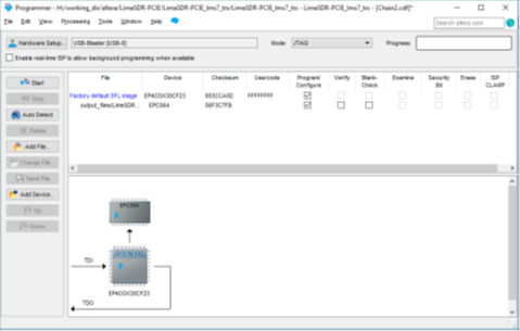
- Apply settings as in Figure 10 and click Start.
- After successful programming turn off computer #1.
- FPGA boots from programmed FLASH memory automatically when computer #1 is turned on.
Obtaining FPGA programming files
FPGA gateware programming file can be obtained by compiling provided LimeSDR-QPCIE_lms7_trx project with Intel Quartus Prime software. Software version used with this guide: Quartus prime 15.1.2 Build 193 02/01/2016 SJ Lite Edition. Quartus Prime Lite Edition software can be downloaded from here.
PCIe core generation
PCIe Xillybus core has to be generated and downloaded in order to compile LimeSDR-QPCIE_lms7_trx FPGA project. This chapter describes steps and parameters required to generate Xillybus PCIe core.
Signing UP
Xillybus requires to fill up free registration form in order to download generated core. Go to link, fill required fields (Figure 11) and confirm registration via received eMail.

Creating new IP core
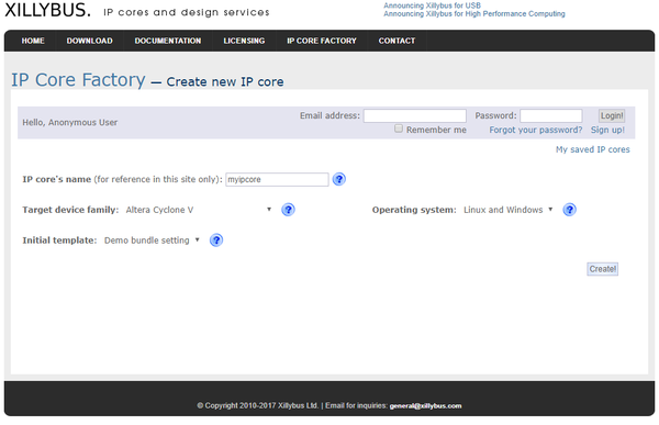
After successful registration, go to IP core Factory page link fill parameters as shown in Figure 12 and click Create!.
Setting core parameters
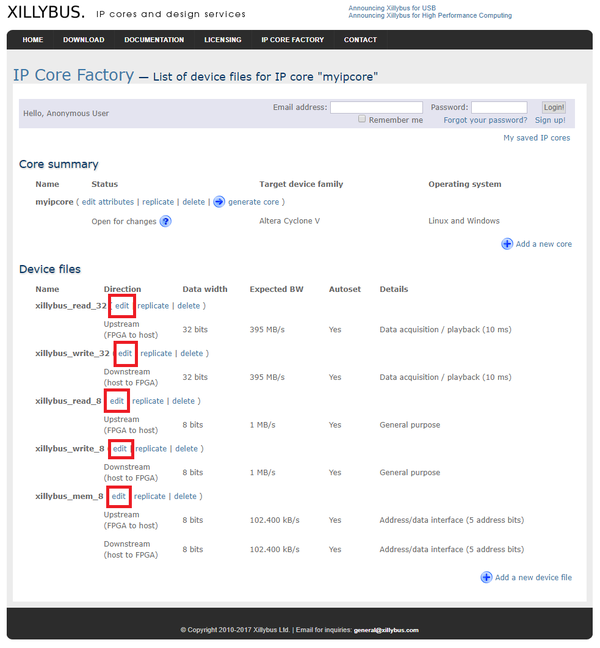
After new core creation in next dialog click Edit to change settings for each device files (Figure 13).
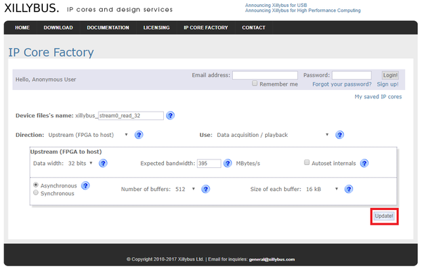
In Edit dialog (Figure 14) fill following parameters for corresponding file and click Update!. To enter all parameters Autoset internals has to be unchecked:
For xillybus_read_32:
•	Device file's name		- stream0_read_32
•	Direction 			- Upstream (FPGA to host)
•	Use 				- Data acquisition / playback
•	Data width			- 32 bits
•	Expected bandwidth		- 395
•	Autoset internals		- unchecked
•	Asynchronous/synchronous 	- Asynchronous
•	Number of buffers		- 512
•	Size of each buffer		- 16 kB
Edit rest of the files with following parameters: For xillybus_write_32: • Device file's name - stream0_write_32 • Direction - Downstream (host to FPGA) • Use - Data acquisition / playback • Data width - 32 bits • Expected bandwidth - 395 • Autoset internals - unchecked • Asynchronous/synchronous - Asynchronous • Number of buffers - 512 • Size of each buffer - 16 kB • DMA acceleration - 8 segments x 512 bytes For xillybus_read_8: • Device file's name - control0_read_32 • Direction - Upstream (FPGA to host) • Use - General purpose • Data width - 32 bits • Expected bandwidth - 1 • Autoset internals - checked For xillybus_write_8: • Device file's name - control0_write_32 • Direction - Downstream (host to FPGA) • Use - General purpose • Data width - 32 bits • Expected bandwidth - 1 • Autoset internals - checked For xillybus_mem_8: • Device file's name - mem_8 • Direction - Bidirectional • Use - Address/data interface (5 address bits) Upstream (FPGA to host) o Data width - 8 bits o Expected bandwidth - 0.1 o Autoset internals - checked Downstream (host to FPGA) o Data width - 8 bits o Expected bandwidth - 0.1 o Autoset internals - checked
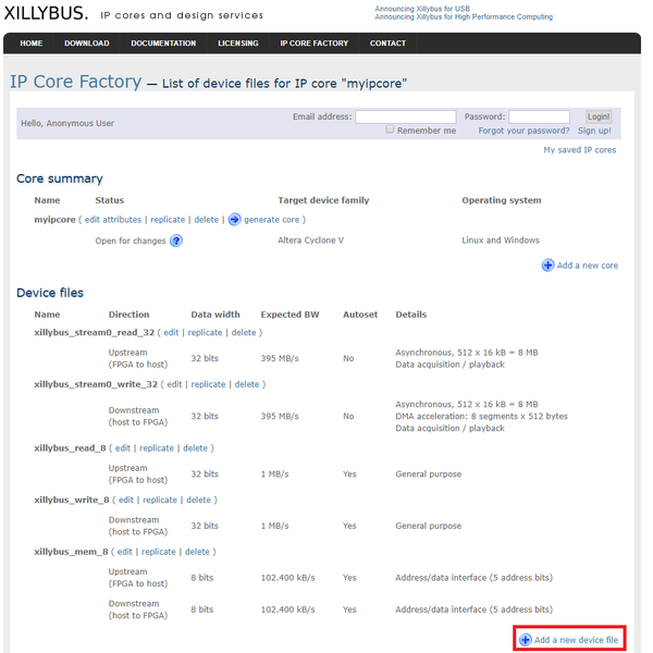
Next step is to add more device files, click Add new device file Figure 15 and add following device files with following parameters:
xillybus_stream1_read_32:
•	Device file's name		- stream1_read_32
•	Direction 			- Upstream (FPGA to host)
•	Use 				- Data acquisition / playback
•	Data width			- 32 bits
•	Expected bandwidth		- 395
•	Autoset internals		- unchecked
•	Asynchronous/synchronous 	- Asynchronous
•	Number of buffers		- 512
•	Size of each buffer		- 16 kB

xillybus_ stream1_write_32:
•	Device file's name 		- stream1_write_32
•	Direction 			- Downstream (host to FPGA)
•	Use 				- Data acquisition / playback
•	Data width			- 32 bits
•	Expected bandwidth		- 395
•	Autoset internals		- unchecked
•	Asynchronous/synchronous 	- Asynchronous
•	Number of buffers		- 512
•	Size of each buffer		- 16 kB
•	DMA acceleration		- 8 segments x 512 bytes

xillybus_stream2_read_32:
•	Device file's name		- stream2_read_32
•	Direction 			- Upstream (FPGA to host)
•	Use 				- Data acquisition / playback
•	Data width			- 32 bits
•	Expected bandwidth		- 395
•	Autoset internals		- unchecked
•	Asynchronous/synchronous 	- Asynchronous
•	Number of buffers		- 512
•	Size of each buffer		- 16 kB

xillybus_stream2_write_32:
•	Device file's name 		- stream2_write_32
•	Direction 			- Downstream (host to FPGA)
•	Use 				- Data acquisition / playback
•	Data width			- 32 bits
•	Expected bandwidth		- 395
•	Autoset internals		- unchecked
•	Asynchronous/synchronous 	- Asynchronous
•	Number of buffers		- 512
•	Size of each buffer		- 16 kB
•	DMA acceleration		- 8 segments x 512 bytes
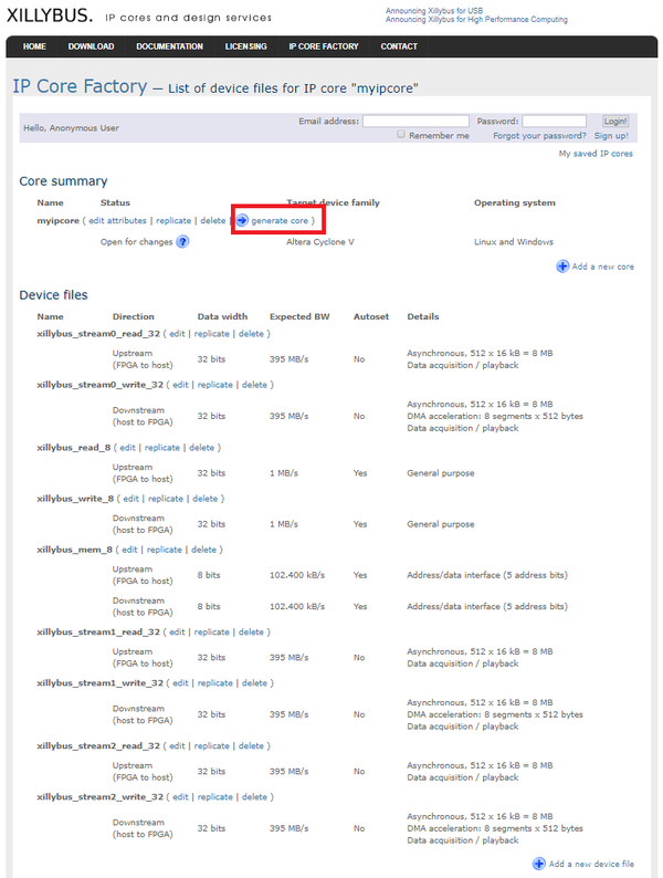
After updating all files click generate core (Figure 16). Check core status and download it when available (Figure 17).

Adding PCIe core to project
This chapter describes steps to include Xillybus core to Quartus project:
- Extract downloaded .zip file “corebundle-myipcore_demo.zip” (myipcore_demo – name that was entered during core generation).
- Place file xillybus.v to Quartus project directory limesdr-qpcie_xillybus_core/
- Place file xillybus_core.qxp to Quartus project directory limesdr-qpcie_xillybus_core/
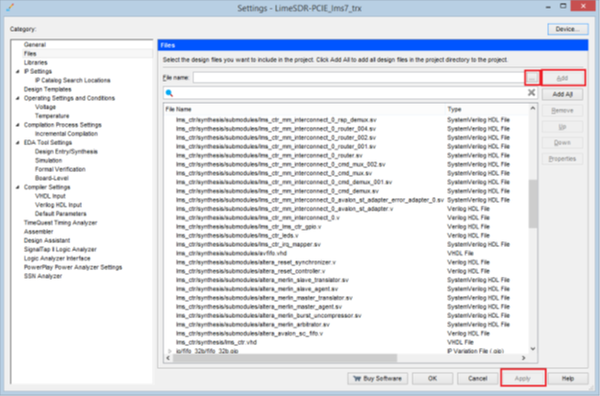
- Open Quartus LimeSDR-QPCIE_lms7_trx project and select Project→ Add/Remove Files in Project.. and add files xillybus.v and xillybus_core.qxp to Quartus project (Figure 82).
- Recompile project Processing → Start Compilation.
Programming files
After performing full project compilation in Quartus prime software Processing → Start Compilation in Messages window (see Figure 19) should appear messages stating that programming files are created:

Programming files can be found in folder output_files from project directory:
- .jic - JTAG Indirect Configuration File can be used to program FPGA gateware to FLASH memory (if valid file is loaded FPGA boots from FLASH when board power is applied automatically).
- .sof - SRAM Object File can be used to program FPGA (has to be programmed every time after board power is applied)
- .rbf - Raw Binary File can be used to program FPGA gateware into FLASH memory through LimeSuiteGUI (valid gateware has to be already running)