LimeSDR-QPCIe v1.2 hardware description
Introduction
LimeSDR-QPCIe is low-cost software defined radio board based on Lime LMS7002M Field Programmable Radio Frequency (FPRF) transceiver and Altera Cyclone V PFGA, through which apps can be programmed to support any type of wireless standard, e.g. UMTS, LTE, LoRa, GPS, WiFi, Zigbee, RFID, Digital Broadcastimng, Radar and many more.
LimeSDR-QPCIe Board Key Features
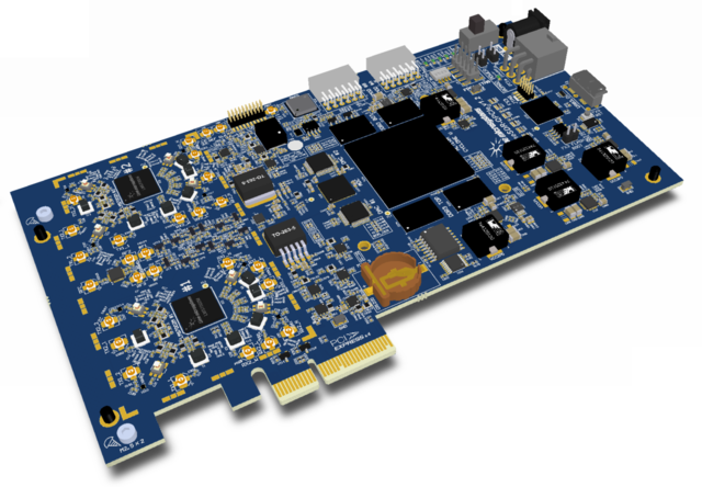
The LimeSDR-QPCIe development board provides a hardware platform for developing and prototyping high-performance and logic-intensive digital and RF designs using Altera’s Cyclone V FPGA and Lime Microsystems transceiver.
For more information on the following topics, refer to the respective documents:
- Cyclone V device family, refer to Cyclone V Device support resources link
- LMS7002M transceiver resources link
LimeSDR-QPCIe v1.2 board features:
- USB Interface
- Cypress FX3 Super Speed USB 3rd generation controller
- FPGA Features
- Cyclone V, 5CGXFC7D7F31C8N device in 896-pin FBGA package
- 150’000 logic elements
- 6860 Kbits embedded memory
- 312 embedded 18x18 multipliers
- 7 PLLs
- 9 Transceivers (2.5Gbps)
- PCIe Hard IP Blocks
- 2 Hard Memory Controllers
- FPGA Configuration
- JTAG mode configuration
- Active serial mode configuration
- Possibility to update FPGA gateware by using FX3 (USB)
- Possibility to update FPGA gateware by using PCIe interface.
- RF
- 2x LMS7002M, FPRF transceivers
- Onboard RSSI measurement circuits
- Onboard loopback control switches
- DACs and ADCs
- 2x DAC5672A, dual, 14-bit, Digital-To-Analog converters
- 1x ADS424, Dual-Channel, 14-bit, Analog-To-Digital converter
- Memory Devices
- 4 x 2Gbit DDR3 SDRAM (128M x 16)
- 4Mbit flash for FX3 firmware
- 128Mbit flash for FPGA gateware
- 2 x 128Kbit and 2 x 512Kbit EEPROMs for LMS MCU firmware, LMS MCU data
- 1 x 128K EEPROM for FX3 or FPGA data
- Connections
- microUSB3.0 (type B) connector
- PCIe x4 edge connector (Gen1)
- Coaxial RF (U.FL) connectors
- 2x PMOD header (0.1” pitch)
- FPGA (0.1” pitch) and FX3 (0.05” pitch) JTAG connectors
- 12V DC power jack and pinheader
- LVDS connector (0.05” pitch)
- Fan connector (12V/5V)
- PCIe 6-pin power connector
- Holder for coin cell CR1220 battery
- Clock System
- 30.72MHz VCTCXO (precision: ±1 ppm initial, ±4 ppm stable).
- Possibility to lock VCTCXO to external clock using ADF4002 or tune VCTCXO by onboard DAC (AD5662)
- Programmable clock generator for the FPGA reference clock input or LMS PLLs
- VCTCXO clock output for external device synchronization.
- 1x 100 MHz, 4 x 125MHz crystal oscillators for FPGA
- Miscellaneous devices
- LM75 Digital temperature sensor with 2-Wire Interface.
- DS3231 real-time clock.
- M0578-A3 GPS/GNSS module receiver
- Board Size 190mm x 106.7mm (7.48” x 4.20”)
LimeSDR-QPCIe Board Overview
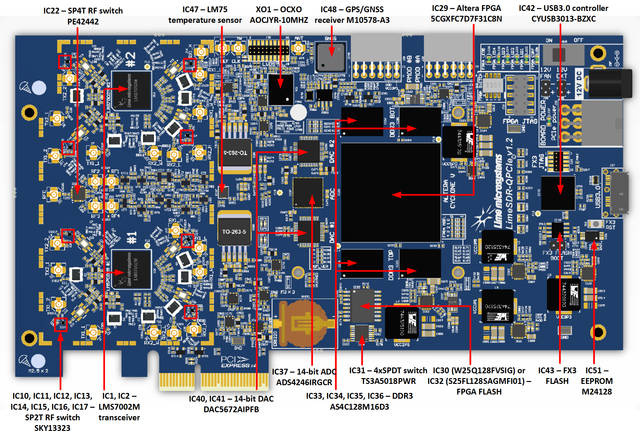
LimeSDR-QPCIe board version 1.2 picture with highlighted major connectors presented in Figure 2. There are three connector types – data and debugging (PCIe, USB3.0, PMOD, LVDS and JTAG), power (DC jack and external supply pinheaders) and high frequency (RF and reference clock).
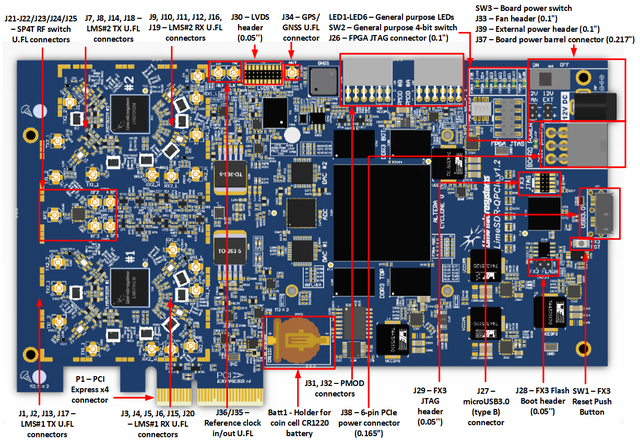
Board components description listed in the Table 1.
| Featured Devices | ||
|---|---|---|
| Board Reference | Type | Description |
| IC1, IC2 | FPRF | Field programmable RF transceivers LMS7002M |
| IC8 | FPGA | Altera Cyclone V GX, 5CGXFC7D7F31C8N, 896-BGA |
| IC13 | USB3.0 microcontroller | Cypress FX3 Supper Speed USB 3rd generation controller CYUSB3013 |
| Miscellaneous devices on board | ||
| IC7, IC8 | IC | 8-bit shift registers 74HC595BQ,115 |
| IC9, IC49 | IC | Bidirectional voltage shifters SN74AVC4T774RSVR |
| IC10, IC11, IC12, IC13, IC14, IC15, IC16, IC17 | IC | 100MHz – 3 GHz SPDT RF switches SKY13323-378LF |
| IC18, IC20, IC23, IC25, IC26, IC28 | IC | 12-bit ADCs MAX11108AVB+T |
| IC19, IC24, IC27 | IC | 1MHz–10GHz dual log detector/controller ADL5519 |
| IC22 | IC | SP4T RF switch PE42442A-Z |
| IC31 | IC | 4 parallel 2:1 switches TS3A5018PWR |
| IC37 | IC | 14-bit 2-channel ADC ADS4246IRGCT |
| IC38 | IC | Dual differential amplifier ADA4930 |
| IC39, IC56 | IC | Differential line drivers SN65LVDS1DBVR |
| IC40, IC41 | IC | Dual differential DACs DAC5672AIPFB |
| IC44, IC45 | IC | Bidirectional 8-channel voltage translators FXLA108BQX |
| IC47 | IC | Temperature sensor LM75 |
| IC48 | IC | GPS receiver module M10578-A3 |
| IC50 | IC | Real time clock (RTC) DS3231S# |
| BATT1 | Holder | Holder for coin cell CR1220 battery |
| ESD26 | TVS | USB3.0 ESD protection TVS diode |
| ESD1, ESD2, ESD3, ESD4, ESD5, ESD6, ESD7, ESD8, ESD9, ESD10, ESD11, ESD12, ESD13, ESD14, ESD15, ESD16, ESD17, ESD18, ESD19, ESD20, ESD21, ESD22, ESD23, ESD24, ESD25 | TVS | RF connector ESD protection TVS diodes |
| Configuration, Status and Setup Components | ||
| R56, R57, R58, R59 | 0 Ohm resistor | Board BOM version BOM_VER[3:0]. Default BOM_VER=0 (all resistors populated). |
| R160, R161, R163, R164, R166, R167, R168, R169, R171, R172 | 0 Ohm resistor | FPGA (IC8) MSEL[3:0]. Default mode: Active Serial Standard configuration. |
| [R268, R271, R275, R279], [R269, R273, R277, R281] | 0 Ohm resistor | DAC#1 differential channels TX1_BB_I/Q connection selection to either LMS7002M #1 or LMS7002M #2. Default populated group is [R268, R271, R275, R279]. Resistor groups are defined in [] brackets. |
| [R270, R274, R278, R282], [R272, R276, R280, R283] | 0 Ohm resistor | DAC#2 differential channels TX2_BB_I/Q connection selection to either LMS7002M #1 or LMS7002M #2. Default populated group is [R270, R274, R278, R282]. Resistor groups are defined in [] brackets. |
| R364, R379, R384 and their respective power connecting resistors R365, R380, R382 | 0 Ohm resistor | Clock buffer (IC52) CLKin0 (pin 13) clock source selection. R364 and R365 are populated by default. |
| R368, R372, R374 | 0 Ohm resistor | Clock buffer (IC52) CLKin1 (pin 28) clock source selection. R374 is populated by default. |
| R375 | 0 Ohm resistor | Clock buffer (IC52) source (CLKin0 or CLKin1) selection. If unpopulated, clock source is CLKin0 (default). If populated, clock source is CLKin1. |
| R302, R305, R307 | 10 kOhm resistor | USB3.0 microcontroller (IC13) boot configuration (PMODE0[2:0]) resistors. Default mode: SPI boot, On Failure - USB Boot |
| R294, R296, R298 | 10 kOhm resistor | USB3.0 microcontroller (IC13) crystal/clock frequency selection (FSLC[2:0]) resistors. Default mode: 19.2MHz crystal |
| J28, R313 | Pin header, 0 Ohm resistor | USB3.0 microcontroller (IC13) boot source (Flash memory or USB), 0.1” pitch jumper or 0402 0R resistor. In normal operation jumper or resistor must be placed. |
| J29 | JTAG chain pin header | USB3.0 microcontroller (IC13) debugging pin header, 0.05” pitch |
| SW1 | Push-button | USB3.0 microcontroller reset button |
| J26 | JTAG chain pin header | FPGA programming pin header for Altera USB-Blaster download cable, 0.1” pitch |
| LED1 | Green status LED | FPGA configuration done LED |
| LED2-LED5 | Green status LEDs | User defined general purpose green LEDs |
| LED6 | Red-green status LED | User defined general purpose dual colour LED |
| General User Input/Output | ||
| J31, J32 | Connector 0.1” | PMOD connectors |
| SW2 | Switch | 4-bit FPGA switch |
| J33 | Pin header | Board cooling fan pin header, 0.1” |
| Memory Devices | ||
| IC3, IC5, IC51 | EEPROM | 128Kbit (16K x 8) EEPROM, LMS7002 MCU firmware and general purpose memory |
| IC4, IC6 | EEPROM | 512Kbit (64K x 8) EEPROM, connected to main I2C bus |
| IC30 | Flash memory | 128Mbit (16M x 8) Flash for FPGA configuration (unpopulated) |
| IC32 | Flash memory | 128Mbit (16M x 8) Flash for FPGA configuration |
| IC33, IC34, IC35, IC36 | DDR3 memory | 2Gbit (128M x 16) DDR3 SDRAM |
| Communication Ports | ||
| J27 | USB3.0 connector | microUSB3.0 (type B) connector |
| P1 | PCIe connector | PCI Express (Gen1) x4 connector |
| Clock Circuitry | ||
| XO1 | VCOCXO | 10MHz voltage- and oven-controlled crystal oscillator |
| XO2, XO3 | VCTCXO | 30.72MHz voltage-controlled crystal oscillator |
| XO4 | VCTCXO | 40MHz voltage-controlled crystal oscillator |
| IC57 | IC | Programmable clock generator for the FPGA reference clock input and RF boards |
| IC53 | IC | ADF4002 phase detector |
| IC54 | IC | 16-bit DAC for VCTCXO/VCOCXO frequency tuning |
| IC52 | IC | Clock buffer |
| IC55 | IC | Clock buffer |
| J36 | U.FL connector | Reference clock input |
| J35 | U.FL connector | Reference clock output |
| XO5 | Crystal oscillator | 100MHz single-ended FPGA clock |
| XO6 | Crystal oscillator | 125MHz single-ended FPGA clock |
| XO7 | Crystal oscillator | 125MHz differential FPGA-DDR clock |
| XO8 | Crystal oscillator | 125MHz differential FPGA-DDR clock |
| XO9 | Crystal oscillator | 125MHz differential FPGA clock for PCIe REFCLK1 |
| IC56 | IC | Single-ended to differential clock converter. Clock source is IC57 pin 9. Connected to FPGA PCIe REFCLK2 and LVDS connector J30. |
| Power Supply | ||
| J37 | DC input jack | External 12V DC power supply |
| J38 | Header | 6-pin PCIe power connector, 0.165” pitch |
| J39 | Pin header | External 12V DC power supply and main internal power rail |
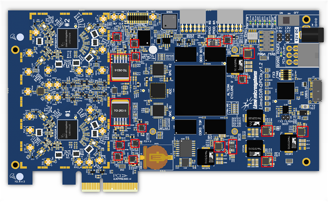
LimeSDR-QPCIe board version 1.2 picture with highlighted top components are presented in Figure 3.
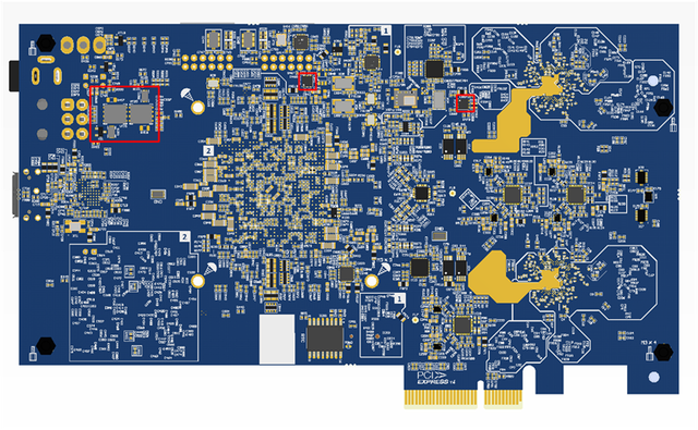
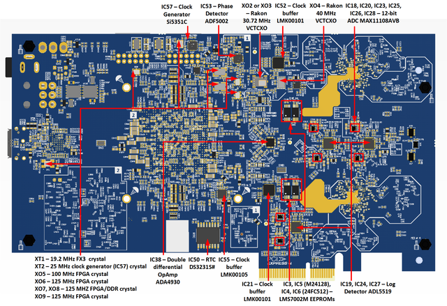
LimeSDR-QPCIe board version 1.2 picture with highlighted bottom components is presented in Figure 4.
LimeSDR-QPCIe Board Architecture
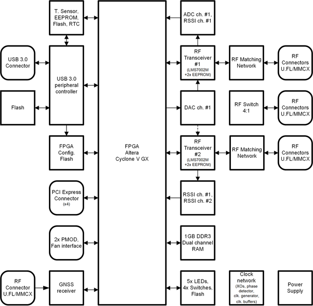
The heart of the LimeSDR-QPCIe board is Altera Cyclone V GX FPGA. Its main function is to transfer digital data between the PC through an edge PCIE and a USB3.0 connector. The block diagram for LimeSDR-QPCIe board is presented in the Figure 5.
FPGA configuration
FPGA is set to use x1 Active Serial (AS) configuration scheme. In this scheme if valid configuration file exists in FLASH memory (IC30 or IC32) it is automatically loaded after power is applied to the board. In Table 2 it is listed resistor setup for Active Serial (AS) configuration mode select.
| Schematic signal name | Logic level | 0R Resistor setup | |
|---|---|---|---|
| MSEL0 | H | R160 (NF) | R161 (Fit) |
| MSEL1 | H | R163 (NF) | R164 (Fit) |
| MSEL2 | L | R166 (Fit) | R167 (NF) |
| MSEL3 | L | R168 (Fit) | R169 (NF) |
| MSEL4 | H | R171 (NF) | R172 (Fit) |
There are two options which allows to change configuration file in FLASH memory:
- USB 3.0 controller – CYUSB3013 (IC42) has access to configuration memory. With valid firmware and software, gateware for FPGA can be uploaded into FLASH memory (IC30 or IC32) by using USB3.0 cable. IC42 can initiate FPGA reconfiguration. For signal interconnect details see chapter 2.2.2.3 USB 3.0 Controller.
- JTAG Header – 10pin connector (J26) provides access to FPGA JTAG chain. By using external download cable such as USB-Blaster and Quartus II Programmer software FLASH memory (IC30 or IC32) can be reprogrammed. JTAG connections are listed in Table 3.
| Connector pin | Schematic signal name | FPGA pin (IC29) | Comment |
|---|---|---|---|
| 1 | FPGA_JTAG_TCK | AC7 | R170 Pull-Down resistor |
| 2 | VCC2P5 | - | |
| 3 | FPGA_JTAG_TDO | W9 | |
| 4 | VCC2P5 | - | |
| 5 | FPGA_JTAG_TMS | V7 | R162 Pull-Up resistor |
| 6 | - | - | |
| 7 | - | - | |
| 8 | - | - | |
| 9 | FPGA_JTAG_TDI | U7 | R165 Pull-Up resistor |
| 10 | GND | - |
Main components
This chapter describes main components mounted on LimeSDR-QPCIe v1.2 board.
LMS7002M RF transceiver
There are two LMS7002M field programmable RF transceiver ICs (LMS7002M#1 - IC1 and LMS7002M#1 - IC2), interface signals can be acknowledged by corresponding names LMSx_*, where x can be 1 or 2. For example LMS1_* signals belongs to IC1 and LMS2_* belongs to IC2.
In the following manner interface and control signals are described below:
- Digital Interface Signals: LMS7002 is using data bus LMSx_DIQ1_D[11:0] and LMSx_DIQ2_D[11:0], LMSx_ENABLE_IQSEL1 and LMSx_ENABLE_IQSEL2, LMSx_FCLK1 and LMSx_FCLK2, LMSx_MCLK1 and LMSx_MCLK2 signals to transfer data to/from FPGA. Indexes 1 and 2 indicate transceiver digital data PORT-1 or PORT-2. Any of these ports can be used to transmit or receive data. By default, PORT-1 is selected as receive port and PORT-2 is selected as transmit port. The FCLK# is input clock and MCLK# is output clock for LMS7002M transceiver. TXNRX signals sets ports directions. For LMS7002M interface timing details refer to LMS7002M transceiver datasheet page 12-13 [1].
- LMS Control Signals: these signals are used for optional functionality:
- LMSx_RXEN, LMSx_TXEN – receiver and transmitter enable/disable signals.
- LMS_RESET – LMS7002M reset signal.
- SPI Interface: LMS7002M transceiver is configured via 4-wire SPI interface; FPGA_SPI0_SCLK, FPGA_SPI0_MOSI, FPGA_SPI0_MISO_LMSx, FPGA_SPI0_LMSx_SS. The SPI interface controlled from FPGA.
- LMS I2C Interface: LMS EEPROM are connected to this interface. The signals LMSx_I2C_SCL, LMSx_I2C_DATA is not connected to FPGA
The Table 4 and Table 5below lists RF transceiver respectively LMS7002#1 and LMS7002#2 pins, schematic signal names, FPGA interconnections and I/O standard.
| Chip pin (IC1) | Chip reference (IC1) | Schematic signal name | FPGA pin | FPGA I/O standard | Comments |
|---|---|---|---|---|---|
| AM24 | xoscin_rx | LMS1_RxPLL_CLK | NC | 3.3V | Connected to 30.72 MHz clock |
| P34 | MCLK2 | LMS1_MCLK2 | U21 | 2.5V/3.3V | |
| R29 | FCLK2 | LMS1_FCLK2 | Y22 | 2.5V/3.3V | |
| U31 | TXNRX2 | LMS1_TXNRX2 | U26 | 2.5V/3.3V | |
| V34 | RXEN | LMS1_RXEN | Y26 | 2.5V/3.3V | |
| R33 | ENABLE_IQSEL2 | LMS1_ENABLE_IQSEL2 | AA26 | 2.5V/3.3V | |
| H30 | DIQ2_D0 | LMS1_DIQ2_D0 | AC27 | 2.5V/3.3V | |
| J31 | DIQ2_D1 | LMS1_DIQ2_D1 | AB27 | 2.5V/3.3V | |
| K30 | DIQ2_D2 | LMS1_DIQ2_D2 | Y21 | 2.5V/3.3V | |
| K32 | DIQ2_D3 | LMS1_DIQ2_D3 | AA29 | 2.5V/3.3V | |
| L31 | DIQ2_D4 | LMS1_DIQ2_D4 | Y28 | 2.5V/3.3V | |
| K34 | DIQ2_D5 | LMS1_DIQ2_D5 | AC26 | 2.5V/3.3V | |
| M30 | DIQ2_D6 | LMS1_DIQ2_D6 | W27 | 2.5V/3.3V | |
| M32 | DIQ2_D7 | LMS1_DIQ2_D7 | AA25 | 2.5V/3.3V | |
| N31 | DIQ2_D8 | LMS1_DIQ2_D8 | V26 | 2.5V/3.3V | |
| N33 | DIQ2_D9 | LMS1_DIQ2_D9 | AH29 | 2.5V/3.3V | |
| P30 | DIQ2_D10 | LMS1_DIQ2_D10 | V27 | 2.5V/3.3V | |
| P32 | DIQ2_D11 | LMS1_DIQ2_D11 | W28 | 2.5V/3.3V | |
| E5 | xoscin_tx | LMS1_TxPLL_CLK | NC | 3.3V | Connected to 30.72 MHz clock |
| AB34 | MCLK1 | LMS1_MCLK1 | U22 | 2.5V/3.3V | |
| AA33 | FCLK1 | LMS1_FCLK1 | Y30 | 2.5V/3.3V | |
| V32 | TXNRX1 | LMS1_TXNRX1 | U27 | 2.5V/3.3V | |
| U29 | TXEN | LMS1_TXEN | V21 | 2.5V/3.3V | |
| Y32 | ENABLE_IQSEL1 | LMS1_ENABLE_IQSEL1 | U28 | 2.5V/3.3V | |
| AG31 | DIQ1_D0 | LMS1_DIQ1_D0 | T28 | 2.5V/3.3V | |
| AF30 | DIQ1_D1 | LMS1_DIQ1_D1 | Y23 | 2.5V/3.3V | |
| AF34 | DIQ1_D2 | LMS1_DIQ1_D2 | AB28 | 2.5V/3.3V | |
| AE31 | DIQ1_D3 | LMS1_DIQ1_D3 | T29 | 2.5V/3.3V | |
| AD30 | DIQ1_D4 | LMS1_DIQ1_D4 | AA23 | 2.5V/3.3V | |
| AC29 | DIQ1_D5 | LMS1_DIQ1_D5 | V22 | 2.5V/3.3V | |
| AE33 | DIQ1_D6 | LMS1_DIQ1_D6 | V24 | 2.5V/3.3V | |
| AD32 | DIQ1_D7 | LMS1_DIQ1_D7 | Y27 | 2.5V/3.3V | |
| AC31 | DIQ1_D8 | LMS1_DIQ1_D8 | AC24 | 2.5V/3.3V | |
| AC33 | DIQ1_D9 | LMS1_DIQ1_D9 | V25 | 2.5V/3.3V | |
| AB30 | DIQ1_D10 | LMS1_DIQ1_D10 | W22 | 2.5V/3.3V | |
| AB32 | DIQ1_D11 | LMS1_DIQ1_D11 | AA24 | 2.5V/3.3V | |
| U33 | CORE_LDO_EN | LMS1_CORE_LDO_EN | Y25 | 2.5V/3.3V | |
| E27 | RESET | LMS1_RESET | L21 | 2.5V/3.3V | |
| D28 | SEN | FPGA_SPI0_LMS1_SS | V29 | 2.5V/3.3V | SPI interface |
| C29 | SCLK | FPGA_SPI0_SCLK | T25 | 2.5V/3.3V | SPI interface |
| F30 | SDIO | FPGA_SPI0_MOSI | R26 | 2.5V/3.3V | SPI interface |
| F28 | SDO | FPGA_SPI0_MISO_LMS1 | R30 | 2.5V/3.3V | SPI interface |
| D26 | SDA | LMS1_I2C_SDA | - | 2.5V | Connected to EEPROM |
| C27 | SCL | LMS1_I2C_SCL | - | 2.5V | Connected to EEPROM |
| Chip pin (IC2) | Chip reference (IC2) | Schematic signal name | FPGA pin | FPGA I/O standard | Comments |
|---|---|---|---|---|---|
| P34 | MCLK2 | LMS2_MCLK2 | U23 | 2.5V/3.3V | |
| R29 | FCLK2 | LMS2_FCLK2 | AC29 | 2.5V/3.3V | |
| U31 | TXNRX2 | LMS2_TXNRX2 | AC30 | 2.5V/3.3V | |
| V34 | RXEN | LMS2_RXEN | AE25 | 2.5V/3.3V | |
| R33 | ENABLE_IQSEL2 | LMS2_ENABLE_IQSEL2 | AF25 | 2.5V/3.3V | |
| H30 | DIQ2_D0 | LMS2_DIQ2_D0 | AA28 | 2.5V/3.3V | |
| J31 | DIQ2_D1 | LMS2_DIQ2_D1 | AJ30 | 2.5V/3.3V | |
| K30 | DIQ2_D2 | LMS2_DIQ2_D2 | AB29 | 2.5V/3.3V | |
| K32 | DIQ2_D3 | LMS2_DIQ2_D3 | AD24 | 2.5V/3.3V | |
| L31 | DIQ2_D4 | LMS2_DIQ2_D4 | AG28 | 2.5V/3.3V | |
| K34 | DIQ2_D5 | LMS2_DIQ2_D5 | AG27 | 2.5V/3.3V | |
| M30 | DIQ2_D6 | LMS2_DIQ2_D6 | AB26 | 2.5V/3.3V | |
| M32 | DIQ2_D7 | LMS2_DIQ2_D7 | AF24 | 2.5V/3.3V | |
| N31 | DIQ2_D8 | LMS2_DIQ2_D8 | AH30 | 2.5V/3.3V | |
| N33 | DIQ2_D9 | LMS2_DIQ2_D9 | AE23 | 2.5V/3.3V | |
| P30 | DIQ2_D10 | LMS2_DIQ2_D10 | AG29 | 2.5V/3.3V | |
| P32 | DIQ2_D11 | LMS2_DIQ2_D11 | AE26 | 2.5V/3.3V | |
| E5 | xoscin_tx | LMS2_TxPLL_CLK | NC | 3.3V | Connected to 30.72 MHz clock |
| AB34 | MCLK1 | LMS2_MCLK1 | T24 | 2.5V/3.3V | |
| AA33 | FCLK1 | LMS2_FCLK1 | W30 | 2.5V/3.3V | |
| V32 | TXNRX1 | LMS2_TXNRX1 | AF28 | 2.5V/3.3V | |
| U29 | TXEN | LMS2_TXEN | AD27 | 2.5V/3.3V | |
| Y32 | ENABLE_IQSEL1 | LMS2_ENABLE_IQSEL1 | AF29 | 2.5V/3.3V | |
| AG31 | DIQ1_D0 | LMS2_DIQ1_D0 | AD25 | 2.5V/3.3V | |
| AF30 | DIQ1_D1 | LMS2_DIQ1_D1 | AD29 | 2.5V/3.3V | |
| AF34 | DIQ1_D2 | LMS2_DIQ1_D2 | AH27 | 2.5V/3.3V | |
| AE31 | DIQ1_D3 | LMS2_DIQ1_D3 | AE30 | 2.5V/3.3V | |
| AD30 | DIQ1_D4 | LMS2_DIQ1_D4 | AE28 | 2.5V/3.3V | |
| AC29 | DIQ1_D5 | LMS2_DIQ1_D5 | AD30 | 2.5V/3.3V | |
| AE33 | DIQ1_D6 | LMS2_DIQ1_D6 | AJ28 | 2.5V/3.3V | |
| AD32 | DIQ1_D7 | LMS2_DIQ1_D7 | AF26 | 2.5V/3.3V | |
| AC31 | DIQ1_D8 | LMS2_DIQ1_D8 | AE27 | 2.5V/3.3V | |
| AC33 | DIQ1_D9 | LMS2_DIQ1_D9 | AJ29 | 2.5V/3.3V | |
| AB30 | DIQ1_D10 | LMS2_DIQ1_D10 | AD28 | 2.5V/3.3V | |
| AB32 | DIQ1_D11 | LMS2_DIQ1_D11 | AF30 | 2.5V/3.3V | |
| U33 | CORE_LDO_EN | LMS2_CORE_LDO_EN | AD23 | 2.5V/3.3V | |
| E27 | RESET | LMS2_RESET | AA30 | 2.5V/3.3V | |
| D28 | SEN | FPGA_SPI0_LMS2_SS | U29 | 2.5V/3.3V | SPI interface |
| C29 | SCLK | FPGA_SPI0_SCLK | T25 | 2.5V/3.3V | SPI interface |
| F30 | SDIO | FPGA_SPI0_MOSI | R26 | 2.5V/3.3V | SPI interface |
| F28 | SDO | FPGA_SPI0_MISO_LMS2 | V30 | 2.5V/3.3V | SPI interface |
| D26 | SDA | LMS2_I2C_SDA | - | 2.5V | Connected to EEPROM |
| C27 | SCL | LMS2_I2C_SCL | - | 2.5V | Connected to EEPROM |
SDRAM
LimeSDR-QPCIe board has four 2Gb DDR3 SDRAM memory ICs (AS4C128M16D3B-12BCN [link]) which are connected to Cyclone V GX FPGA. The memory can be used for data manipulation at high data rates between transceiver and FPGA. There are two independent DDR3 SDRAM interfaces:
- DDR3 TOP – this is 32bit data interface which consist of two x16 memory devices (IC33 AND IC34) with a single address and command bus. Interface is connected to FPGA Bank 7A and 8A and uses hard memory controller. Error! Reference source not found. lists DDR3 TOP interface pins.
- DDR3 BOT – this is 32bit data interface which consist of two x16 memory devices (IC35 AND IC36) with a single address and command bus. Interface is connected to FPGA Bank 3B and 4A and uses hard memory controller. lists DDR3 BOT interface pins.
Following Table 6 lists signal and pin information for DDR3 TOP interface and Table 7 for the DDR3 BOT interface.
| RAM reference | RAM pin | Schematic signal name | FPGA pin (IC29) | FPGA I/O standard | Comments |
|---|---|---|---|---|---|
| Address bus (IC33 and IC34 shared signals) | |||||
| A0 | N3 | DDR3_TOP_A0 | B11 | SSTL-15 Class I | Active termination |
| A1 | P7 | DDR3_TOP_A1 | A11 | SSTL-15 Class I | Active termination |
| A2 | P3 | DDR3_TOP_A2 | F9 | SSTL-15 Class I | Active termination |
| A3 | N2 | DDR3_TOP_A3 | E10 | SSTL-15 Class I | Active termination |
| A4 | P8 | DDR3_TOP_A4 | F16 | SSTL-15 Class I | Active termination |
| A5 | P2 | DDR3_TOP_A5 | E16 | SSTL-15 Class I | Active termination |
| A6 | R8 | DDR3_TOP_A6 | D9 | SSTL-15 Class I | Active termination |
| A7 | R2 | DDR3_TOP_A7 | C10 | SSTL-15 Class I | Active termination |
| A8 | T8 | DDR3_TOP_A8 | E12 | SSTL-15 Class I | Active termination |
| A9 | R3 | DDR3_TOP_A9 | D13 | SSTL-15 Class I | Active termination |
| A10/AP | L7 | DDR3_TOP_A10 | B7 | SSTL-15 Class I | Active termination |
| A11 | R7 | DDR3_TOP_A11 | A8 | SSTL-15 Class I | Active termination |
| A12/BC# | N7 | DDR3_TOP_A12 | B6 | SSTL-15 Class I | Active termination |
| A13 | T3 | DDR3_TOP_A13 | A6 | SSTL-15 Class I | Active termination |
| Bank address bus (IC33 and IC34 shared signals) | |||||
| BA0 | M2 | DDR3_TOP_BA0 | A10 | SSTL-15 Class I | Active termination |
| BA1 | N8 | DDR3_TOP_BA1 | F15 | SSTL-15 Class I | Active termination |
| BA2 | M3 | DDR3_TOP_BA2 | E15 | SSTL-15 Class I | Active termination |
| Data bus [0:15] (IC33) | |||||
| DQ0 | E3 | DDR3_TOP_DQ0 | C15 | SSTL-15 Class I | |
| DQ1 | F7 | DDR3_TOP_DQ1 | C16 | SSTL-15 Class I | |
| DQ2 | F2 | DDR3_TOP_DQ2 | C11 | SSTL-15 Class I | |
| DQ3 | F8 | DDR3_TOP_DQ3 | A13 | SSTL-15 Class I | |
| DQ4 | H3 | DDR3_TOP_DQ4 | D17 | SSTL-15 Class I | |
| DQ5 | H8 | DDR3_TOP_DQ5 | E17 | SSTL-15 Class I | |
| DQ6 | G2 | DDR3_TOP_DQ6 | D12 | SSTL-15 Class I | |
| DQ7 | H7 | DDR3_TOP_DQ7 | A14 | SSTL-15 Class I | |
| DQ8 | D7 | DDR3_TOP_DQ8 | B17 | SSTL-15 Class I | |
| DQ9 | C3 | DDR3_TOP_DQ9 | C17 | SSTL-15 Class I | |
| DQ10 | C8 | DDR3_TOP_DQ10 | A16 | SSTL-15 Class I | |
| DQ11 | C2 | DDR3_TOP_DQ11 | C14 | SSTL-15 Class I | |
| DQ12 | A7 | DDR3_TOP_DQ12 | F18 | SSTL-15 Class I | |
| DQ13 | A2 | DDR3_TOP_DQ13 | G18 | SSTL-15 Class I | |
| DQ14 | B8 | DDR3_TOP_DQ14 | B18 | SSTL-15 Class I | |
| DQ15 | A3 | DDR3_TOP_DQ15 | A19 | SSTL-15 Class I | |
| Data bus [16:31] (IC34) | |||||
| DQ0 | E3 | DDR3_TOP_DQ16 | D18 | SSTL-15 Class I | |
| DQ1 | F7 | DDR3_TOP_DQ17 | D19 | SSTL-15 Class I | |
| DQ2 | F2 | DDR3_TOP_DQ18 | A21 | SSTL-15 Class I | |
| DQ3 | F8 | DDR3_TOP_DQ19 | B21 | SSTL-15 Class I | |
| DQ4 | H3 | DDR3_TOP_DQ20 | E18 | SSTL-15 Class I | |
| DQ5 | H8 | DDR3_TOP_DQ21 | F19 | SSTL-15 Class I | |
| DQ6 | G2 | DDR3_TOP_DQ22 | B23 | SSTL-15 Class I | |
| DQ7 | H7 | DDR3_TOP_DQ23 | B24 | SSTL-15 Class I | |
| DQ8 | D7 | DDR3_TOP_DQ24 | C19 | SSTL-15 Class I | |
| DQ9 | C3 | DDR3_TOP_DQ25 | D20 | SSTL-15 Class I | |
| DQ10 | C8 | DDR3_TOP_DQ26 | A25 | SSTL-15 Class I | |
| DQ11 | C2 | DDR3_TOP_DQ27 | D22 | SSTL-15 Class I | |
| DQ12 | A7 | DDR3_TOP_DQ28 | C20 | SSTL-15 Class I | |
| DQ13 | A2 | DDR3_TOP_DQ29 | C21 | SSTL-15 Class I | |
| DQ14 | B8 | DDR3_TOP_DQ30 | D23 | SSTL-15 Class I | |
| DQ15 | A3 | DDR3_TOP_DQ31 | C25 | SSTL-15 Class I | |
| Data mask[0:1] (IC33) | |||||
| LDM | E7 | DDR3_TOP_DM0 | B14 | SSTL-15 Class I | |
| UDM | D3 | DDR3_TOP_DM1 | B19 | SSTL-15 Class I | |
| Data mask[2:3] (IC34) | |||||
| LDM | E7 | DDR3_TOP_DM2 | C24 | SSTL-15 Class I | |
| UDM | D3 | DDR3_TOP_DM3 | D25 | SSTL-15 Class I | |
| Data strobe[0:1] (IC33) | |||||
| LDQS | G3 | DDR3_TOP_DQS0_P | K17 | Differential 1.5-V SSTL Class I | |
| LDQS# | F3 | DDR3_TOP_DQS0_N | J17 | Differential 1.5-V SSTL Class I | |
| UDQS | C7 | DDR3_TOP_DQS1_P | K16 | Differential 1.5-V SSTL Class I | |
| UDQS# | B7 | DDR3_TOP_DQS1_N | L16 | Differential 1.5-V SSTL Class I | |
| Data strobe[2:3] (IC34) | |||||
| LDQS | G3 | DDR3_TOP_DQS2_P | L18 | Differential 1.5-V SSTL Class I | |
| LDQS# | F3 | DDR3_TOP_DQS2_N | K18 | Differential 1.5-V SSTL Class I | |
| UDQS | C7 | DDR3_TOP_DQS3_P | K20 | Differential 1.5-V SSTL Class I | |
| UDQS# | B7 | DDR3_TOP_DQS3_N | J19 | Differential 1.5-V SSTL Class I | |
| Memory clock (IC33 and IC34 shared signals) | |||||
| CK# | K7 | DDR3_TOP_CK_N | M8 | Differential 1.5-V SSTL Class I | |
| CK | J7 | DDR3_TOP_CK_P | M9 | Differential 1.5-V SSTL Class I | |
| Control signals(IC33 and IC34 shared signals) | |||||
| CKE | K9 | DDR3_TOP_CKE | A18 | SSTL-15 Class I | |
| WE# | L3 | DDR3_TOP_WEn | C7 | SSTL-15 Class I | Active termination |
| CAS# | K3 | DDR3_TOP_CASn | C9 | SSTL-15 Class I | Active termination |
| RAS# | J3 | DDR3_TOP_RASn | B8 | SSTL-15 Class I | Active termination |
| CS# | L2 | DDR3_TOP_CSn | J15 | SSTL-15 Class I | Active termination |
| ODT | K1 | DDR3_TOP_ODT | B13 | SSTL-15 Class I | Active termination |
| RESET# | T2 | DDR3_TOP_RESETn | B22 | 1.5V | Active termination |
| VREF (IC33 and IC34 shared signals) | |||||
| VREFDQ | H1 | VREF_DDR3_TOP | - | ||
| VREFCA | M8 | VREF_DDR3_TOP | - | ||
| Memory ZQ impedance calibration (IC33) | |||||
| ZQ | L8 | DDR3_TOP_RZQ0 | - | ||
| Memory ZQ impedance calibration (IC34) | |||||
| ZQ | L8 | DDR3_TOP_RZQ1 | - | ||
| FPGA OCT calibration pin | |||||
| - | - | OCT_RZQIN1 | B12 | SSTL-15 | |
| RAM reference | RAM pin | Schematic signal name | FPGA pin (IC29) | FPGA I/O standard | Comments |
|---|---|---|---|---|---|
| Address bus (IC35 and IC36 shared signals) | |||||
| A0 | N3 | DDR3_BOT_A0 | AJ12 | SSTL-15 Class I | Active termination |
| A1 | P7 | DDR3_BOT_A1 | AK12 | SSTL-15 Class I | Active termination |
| A2 | P3 | DDR3_BOT_A2 | AH11 | SSTL-15 Class I | Active termination |
| A3 | N2 | DDR3_BOT_A3 | AH12 | SSTL-15 Class I | Active termination |
| A4 | P8 | DDR3_BOT_A4 | AG13 | SSTL-15 Class I | Active termination |
| A5 | P2 | DDR3_BOT_A5 | AG14 | SSTL-15 Class I | Active termination |
| A6 | R8 | DDR3_BOT_A6 | AK10 | SSTL-15 Class I | Active termination |
| A7 | R2 | DDR3_BOT_A7 | AK11 | SSTL-15 Class I | Active termination |
| A8 | T8 | DDR3_BOT_A8 | AF11 | SSTL-15 Class I | Active termination |
| A9 | R3 | DDR3_BOT_A9 | AG11 | SSTL-15 Class I | Active termination |
| A10/AP | L7 | DDR3_BOT_A10 | AJ8 | SSTL-15 Class I | Active termination |
| A11 | R7 | DDR3_BOT_A11 | AK8 | SSTL-15 Class I | Active termination |
| A12/BC# | N7 | DDR3_BOT_A12 | AJ7 | SSTL-15 Class I | Active termination |
| A13 | T3 | DDR3_BOT_A13 | AK7 | SSTL-15 Class I | Active termination |
| Bank address bus (IC35 and IC36 shared signals) | |||||
| BA0 | M2 | DDR3_BOT_BA0 | AH9 | SSTL-15 Class I | Active termination |
| BA1 | N8 | DDR3_BOT_BA1 | AH10 | SSTL-15 Class I | Active termination |
| BA2 | M3 | DDR3_BOT_BA2 | AJ10 | SSTL-15 Class I | Active termination |
| Data bus [0:15] (IC35) | |||||
| DQ0 | E3 | DDR3_BOT_DQ0 | AF15 | SSTL-15 Class I | |
| DQ1 | F7 | DDR3_BOT_DQ1 | AE16 | SSTL-15 Class I | |
| DQ2 | F2 | DDR3_BOT_DQ2 | AJ14 | SSTL-15 Class I | |
| DQ3 | F8 | DDR3_BOT_DQ3 | AH15 | SSTL-15 Class I | |
| DQ4 | H3 | DDR3_BOT_DQ4 | AE17 | SSTL-15 Class I | |
| DQ5 | H8 | DDR3_BOT_DQ5 | AD17 | SSTL-15 Class I | |
| DQ6 | G2 | DDR3_BOT_DQ6 | AJ15 | SSTL-15 Class I | |
| DQ7 | H7 | DDR3_BOT_DQ7 | AF14 | SSTL-15 Class I | |
| DQ8 | D7 | DDR3_BOT_DQ8 | AK17 | SSTL-15 Class I | |
| DQ9 | C3 | DDR3_BOT_DQ9 | AK16 | SSTL-15 Class I | |
| DQ10 | C8 | DDR3_BOT_DQ10 | AG17 | SSTL-15 Class I | |
| DQ11 | C2 | DDR3_BOT_DQ11 | AJ18 | SSTL-15 Class I | |
| DQ12 | A7 | DDR3_BOT_DQ12 | AG16 | SSTL-15 Class I | |
| DQ13 | A2 | DDR3_BOT_DQ13 | AF16 | SSTL-15 Class I | |
| DQ14 | B8 | DDR3_BOT_DQ14 | AJ19 | SSTL-15 Class I | |
| DQ15 | A3 | DDR3_BOT_DQ15 | AH20 | SSTL-15 Class I | |
| Data bus [16:31] (IC36) | |||||
| DQ0 | E3 | DDR3_BOT_DQ16 | AE18 | SSTL-15 Class I | |
| DQ1 | F7 | DDR3_BOT_DQ17 | AD18 | SSTL-15 Class I | |
| DQ2 | F2 | DDR3_BOT_DQ18 | AJ20 | SSTL-15 Class I | |
| DQ3 | F8 | DDR3_BOT_DQ19 | AK22 | SSTL-15 Class I | |
| DQ4 | H3 | DDR3_BOT_DQ20 | AF19 | SSTL-15 Class I | |
| DQ5 | H8 | DDR3_BOT_DQ21 | AF18 | SSTL-15 Class I | |
| DQ6 | G2 | DDR3_BOT_DQ22 | AH21 | SSTL-15 Class I | |
| DQ7 | H7 | DDR3_BOT_DQ23 | AK23 | SSTL-15 Class I | |
| DQ8 | D7 | DDR3_BOT_DQ24 | AG19 | SSTL-15 Class I | |
| DQ9 | C3 | DDR3_BOT_DQ25 | AG18 | SSTL-15 Class I | |
| DQ10 | C8 | DDR3_BOT_DQ26 | AH24 | SSTL-15 Class I | |
| DQ11 | C2 | DDR3_BOT_DQ27 | AK25 | SSTL-15 Class I | |
| DQ12 | A7 | DDR3_BOT_DQ28 | AE20 | SSTL-15 Class I | |
| DQ13 | A2 | DDR3_BOT_DQ29 | AD19 | SSTL-15 Class I | |
| DQ14 | B8 | DDR3_BOT_DQ30 | AG24 | SSTL-15 Class I | |
| DQ15 | A3 | DDR3_BOT_DQ31 | AK26 | SSTL-15 Class I | |
| Data mask[0:1] (IC35) | |||||
| LDM | E7 | DDR3_BOT_DM0 | AE15 | SSTL-15 Class I | |
| UDM | D3 | DDR3_BOT_DM1 | AH19 | SSTL-15 Class I | |
| Data mask[2:3] (IC36) | |||||
| LDM | E7 | DDR3_BOT_DM2 | AJ23 | SSTL-15 Class I | |
| UDM | D3 | DDR3_BOT_DM3 | AJ27 | SSTL-15 Class I | |
| Data strobe[0:1] (IC35) | |||||
| LDQS | G3 | DDR3_BOT_DQS0_P | Y16 | Differential 1.5-V SSTL Class I | |
| LDQS# | F3 | DDR3_BOT_DQS0_N | AA16 | Differential 1.5-V SSTL Class I | |
| UDQS | C7 | DDR3_BOT_DQS1_P | Y17 | Differential 1.5-V SSTL Class I | |
| UDQS# | B7 | DDR3_BOT_DQS1_N | Y18 | Differential 1.5-V SSTL Class I | |
| Data strobe[2:3] (IC36) | |||||
| LDQS | G3 | DDR3_BOT_DQS2_P | Y20 | Differential 1.5-V SSTL Class I | |
| LDQS# | F3 | DDR3_BOT_DQS2_N | AA20 | Differential 1.5-V SSTL Class I | |
| UDQS | C7 | DDR3_BOT_DQS3_P | AB19 | Differential 1.5-V SSTL Class I | |
| UDQS# | B7 | DDR3_BOT_DQS3_N | AC19 | Differential 1.5-V SSTL Class I | |
| Memory clock (IC35 and IC36 shared signals) | |||||
| CK# | K7 | DDR3_BOT_CK_N | AA14 | Differential 1.5-V SSTL Class I | |
| CK | J7 | DDR3_BOT_CK_P | Y13 | Differential 1.5-V SSTL Class I | |
| Control signals(IC35 and IC36 shared signals) | |||||
| sCKE | K9 | DDR3_BOT_CKE | AK18 | SSTL-15 Class I | |
| WE# | L3 | DDR3_BOT_WEn | AK5 | SSTL-15 Class I | Active termination |
| CAS# | K3 | DDR3_BOT_CASn | AF9 | SSTL-15 Class I | Active termination |
| RAS# | J3 | DDR3_BOT_RASn | AG9 | SSTL-15 Class I | Active termination |
| CS# | L2 | DDR3_BOT_CSn | Y12 | SSTL-15 Class I | Active termination |
| ODT | K1 | DDR3_BOT_ODT | AH14 | SSTL-15 Class I | Active termination |
| RESET# | T2 | DDR3_BOT_RESETn | AK21 | 1.5V | Active termination |
| VREF (IC35 and IC36 shared signals) | |||||
| VREFDQ | H1 | VREF_DDR3_BOT | - | ||
| VREFCA | M8 | VREF_DDR3_BOT | - | ||
| Memory ZQ impedance calibration (IC35) | |||||
| ZQ | L8 | DDR3_BOT_RZQ0 | - | ||
| Memory ZQ impedance calibration (IC36) | |||||
| ZQ | L8 | DDR3_BOT_RZQ1 | - | ||
| FPGA OCT calibration pin | |||||
| - | - | OCT_RZQIN0 | AK13 | SSTL-15 | |
USB 3.0 Controller
Software can control LimeSDR-QPCIe board via the USB3 microcontroller (CYUSB3013 (FX3) [link]). The data transfer to/from the board, SPI communication, FPGA configuration is done via the USB3 controller. The controller signals description showed below:
- FX3_DQ[15:0] - FX3 16-bit GPIF data interface is connected FPGA.
- FX3_CTL[12:0] - FX3 GPIF interface control signals.
- FX3_PCLK - GPIF interface clock, connected to FPGA.
- FX3_SPI - interface is used to program FX3 firmware flash or FPGA configuration flash memory.
- FX3 I2C - bus is connected to the main I2C bus.
- PMODE[2:0] – boot options, by default boot from SPI and USB boot is enabled. If J28 jumper is present or R313 is soldered FX3 will boot from IC43 flash memory if correct firmware exists.
- SW1 – resets FX3
- J29 – FX3 JTAG programming/debugging pin header.
In the Table 8 are listed USB3.0 controller (FX3) pins, schematic signal name, FPGA interconnections and I/O standard.
| Chip pin (IC42) | Chip pin (IC42) | Schematic signal name | FPGA pin | FPGA I/O standard | Comments |
|---|---|---|---|---|---|
| F10 | GPIO0 | FX3_DQ0 | U12 | 1.8V | |
| F9 | GPIO1 | FX3_DQ1 | U11 | 1.8V | |
| F7 | GPIO2 | FX3_DQ2 | U8 | 1.8V | |
| G10 | GPIO3 | FX3_DQ3 | U9 | 1.8V | |
| G9 | GPIO4 | FX3_DQ4 | T11 | 1.8V | |
| F8 | GPIO5 | FX3_DQ5 | R10 | 1.8V | |
| H10 | GPIO6 | FX3_DQ6 | T10 | 1.8V | |
| H9 | GPIO7 | FX3_DQ7 | T9 | 1.8V | |
| J10 | GPIO8 | FX3_DQ8 | V11 | 1.8V | |
| J9 | GPIO9 | FX3_DQ9 | V9 | 1.8V | |
| K11 | GPIO10 | FX3_DQ10 | V10 | 1.8V | |
| L10 | GPIO11 | FX3_DQ11 | W10 | 1.8V | |
| K10 | GPIO12 | FX3_DQ12 | Y10 | 1.8V | |
| K9 | GPIO13 | FX3_DQ13 | Y11 | 1.8V | |
| J8 | GPIO14 | FX3_DQ14 | AA11 | 1.8V | |
| G8 | GPIO15 | FX3_DQ15 | AA8 | 1.8V | |
| J6 | GPIO16 | FX3_PCLK | AB16 | 1.5V | |
| K8 | GPIO17 | FX3_CTL0 | AA9 | 1.8V | |
| K7 | GPIO18 | FX3_CTL1 | AB8 | 1.8V | |
| J7 | GPIO19 | FX3_CTL2 | AC9 | 1.8V | |
| H7 | GPIO20 | FX3_CTL3 | AD9 | 1.8V | |
| G7 | GPIO21 | FX3_CTL4 | AF8 | 1.8V | |
| G6 | GPIO22 | FX3_CTL5 | AF7 | 1.8V | |
| K6 | GPIO23 | FX3_CTL6 | AG7 | 1.8V | |
| H8 | GPIO24 | FX3_CTL7 | AF6 | 1.8V | |
| G5 | GPIO25 | FX3_CTL8 | AG6 | 1.8V | |
| H6 | GPIO26 | FX3_CTL9 | AH7 | 1.8V | |
| K5 | GPIO27 | FX3_CTL10 | AH6 | 1.8V | |
| J5 | GPIO28 | FX3_CTL11 | AH4 | 1.8V | |
| H5 | GPIO29 | FX3_CTL12 | AH5 | 1.8V | |
| G4 | GPIO30 | FX3_PMODE0 | - | 1.8V | |
| H4 | GPIO31 | FX3_PMODE1 | - | 1.8V | |
| L4 | GPIO32 | FX3_PMODE2 | - | 1.8V | |
| K2 | GPIO33 | - | - | - | |
| J4 | GPIO34 | - | - | - | |
| K1 | GPIO35 | - | - | - | |
| J2 | GPIO36 | - | - | - | |
| J3 | GPIO37 | - | - | - | |
| J1 | GPIO38 | - | - | - | |
| H2 | GPIO39 | - | - | - | |
| H3 | GPIO40 | - | - | - | |
| F4 | GPIO41 | FPGA_CONF_DONE | L8 | - | Connected to FPGA configuration status CONF_DONE. Additionally, connected to LED1. |
| G2 | GPIO42 | FPGA_NSTATUS | K7 | - | Connected to FPGA nSTATUS pin. |
| G3 | GPIO43 | FPGA_NCONFIG | C5 | - | A high-to-low logic initiates a FPGA reconfiguration. |
| F3 | GPIO44 | FX3_AS_SW | - | - | Logic level L connects FX3_SPI interface to FPGA conf. Flash (IC30, IC32) |
| F2 | GPIO45 | FX3_SPI_AS_SS | - | - | FPGA conf. Flash slave select |
| F5 | GPIO46 | FX3_SPI_FPGA_SS | - | - | |
| E1 | GPIO47 | FX3_FPGA_GPIO0 | AA10 | 1.8V | |
| E5 | GPIO48 | FX3_FPGA_GPIO1 | AB9 | 1.8V | |
| E4 | GPIO49 | FX3_FPGA_GPIO2 | AG8 | 1.8V | |
| D1 | GPIO50 | FX3_FPGA_GPIO3 | AK3 | 1.5V | |
| D2 | GPIO51 | FX3_FPGA_GPIO4 | AJ4 | 1.5V | |
| D3 | GPIO52 | FX3_FPGA_GPIO5 | AJ3 | 1.5V | |
| D4 | GPIO53 | FX3_SPI_SCLK | P20 | 2.5V/3.3V | |
| C1 | GPIO54 | FX3_SPI_FLASH_SS | - | - | Connected to FX3 memory through header J28 |
| C2 | GPIO55 | FX3_SPI_MISO | M21 | 2.5V/3.3V | |
| D5 | GPIO56 | FX3_SPI_MOSI | N20 | 2.5V/3.3V | |
| C4 | GPIO57 | - | - | - | |
| A3 | SSRXM | FX3_USB_SSRX_P | - | - | |
| A4 | SSRXP | FX3_USB_SSRX_N | - | - | |
| A6 | SSTXM | FX3_USB_SSTX_IC_P | - | - | |
| A5 | SSTXP | FX3_USB_SSTX_IC_N | - | - | |
| B3 | R_usb3 | - | - | - | USB3 precision resistor |
| C9 | OTG_ID | FX3_USB_OTG_ID | - | - | |
| A9 | DP | FX3_USB_D_P | - | - | |
| A10 | DM | FX3_USB_D_N | - | - | |
| C8 | R_usb2 | - | - | - | USB2 precision resistor |
| E11 | VBUS | FX3_VBUS | - | - | |
| B2 | FSLC[0] | - | - | - | 10k pulldown for 19.2MHz crystal selection |
| C6 | XTALIN | CYUSB_XTAL_P | - | - | |
| C7 | XTALOUT | CYUSB_XTAL_N | - | - | |
| B4 | FSLC[1] | - | - | - | 10k pulldown for 19.2MHz crystal selection |
| E6 | FSLC[2] | - | - | - | |
| D7 | CLKIN | - | - | - | |
| D6 | CLKIN_32 | - | - | - | |
| D9 | I2C_SCL | FX3_I2C_SCL/ I2C_SCL | AG23 | 1.5V | Voltage level reduced to connect to FPGA. Net labels on FPGA side: I2C_SCL_LS, I2C_SDA_LS |
| D10 | I2C_SDA | FX3_I2C_SDA/ I2C_SDA | AH22 | 1.5V | |
| E7 | TDI | FX3_JTAG_TDI | - | - | 10-pin JTAG connector J29 |
| C10 | TDO | FX3_JTAG_TDO | - | - | |
| B11 | TRST# | FX3_JTAG_TRST | - | - | |
| E8 | TMS | FX3_JTAG_TMS | - | - | |
| F6 | TCK | FX3_JTAG_TCK | - | - | |
| D11 | O[60] | - | - | - |
ADC
There is one Dual-Channel 14-Bit, analog-to-digital converter (ADS4246 – IC37) mounted on board. ADC analog input is connected to RX BB outputs of LMS7002M#1 IC. Digital output pins are connected to FPGA.
The Table 9 lists 14-bit analog to digital converter ADC (IC37) pins, schematic signal name, FPGA interconnections and I/O standard.
| Chip pin (IC37) | Chip reference (IC37) | Schematic signal name | FPGA pin | FPGA I/O standard |
|---|---|---|---|---|
| 41 | DA0_P/DA1 | ADC_DA0_P | L10 | 1.5V |
| 40 | DA0_M/DA0 | ADC_DA0_N | L9 | 1.5V |
| 43 | DA2_P/DA3 | ADC_DA1_P | P10 | 1.5V |
| 42 | DA2_M/DA2 | ADC_DA1_N | N11 | 1.5V |
| 45 | DA4_P/DA5 | ADC_DA2_P | N10 | 1.5V |
| 44 | DA4_M/DA4 | ADC_DA2_N | N9 | 1.5V |
| 47 | DA6_P/DA7 | ADC_DA3_P | R12 | 1.5V |
| 46 | DA6_M/DA6 | ADC_DA3_N | R11 | 1.5V |
| 51 | DA8_P/DA13 | ADC_DA4_P | P12 | 1.5V |
| 50 | DA8_M/DA12 | ADC_DA4_N | N12 | 1.5V |
| 53 | DA10_P/DA9 | ADC_DA5_P | M12 | 1.5V |
| 52 | DA10_M/DA8 | ADC_DA5_N | M11 | 1.5V |
| 55 | DA12_P/DA11 | ADC_DA6_P | L11 | 1.5V |
| 54 | DA12_M/DA10 | ADC_DA6_N | K11 | 1.5V |
| 61 | DB0_P/DB1 | ADC_DB0_P | K12 | 1.5V |
| 60 | DB0_M/DB0 | ADC_DB0_N | J12 | 1.5V |
| 63 | DB2_P/DB3 | ADC_DB1_P | E22 | 1.5V |
| 62 | DB2_M/DB2 | ADC_DB1_N | E21 | 1.5V |
| 3 | DB4_P/DB5 | ADC_DB2_P | E10 | 1.5V |
| 2 | DB4_M/DB4 | ADC_DB2_N | D10 | 1.5V |
| 5 | DB6_P/DB7 | ADC_DB3_P | G14 | 1.5V |
| 4 | DB6_M/DB6 | ADC_DB3_N | F14 | 1.5V |
| 7 | DB8_P/DB13 | ADC_DB4_P | H12 | 1.5V |
| 6 | DB8_M/DB12 | ADC_DB4_N | G12 | 1.5V |
| 9 | DB10_P/DB9 | ADC_DB5_P | J14 | 1.5V |
| 8 | DB10_M/DB8 | ADC_DB5_N | H14 | 1.5V |
| 11 | DB12_P/DB11 | ADC_DB6_P | K13 | 1.5V |
| 10 | DB12_M/DB10 | ADC_DB6_N | J13 | 1.5V |
| 35 | CTRL1 | ADC_CTRL1 | - | - |
| 36 | CTRL2 | ADC_CTRL2 | - | - |
| 34 | CTRL3 | ADC_CTRL3 | - | - |
| 29 | INP_A | ADC_INA_P | - | - |
| 30 | INM_A | ADC_INA_N | - | - |
| 23 | VCM | ADC_VCM | - | - |
| 57 | CLKOUTP/CLKOUT | ADC_CLKOUT_P | L14 | 1.5V |
| 56 | CLKOUTM/UNUSED | ADC_CLKOUT_N | L13 | 1.5V |
| 19 | INP_B | ADC_INB_P | - | - |
| 20 | INM_B | ADC_INB_N | - | - |
| 25 | CLKP | ADC_CLK_P | - | - |
| 26 | CLKM | ADC_CLK_N | - | - |
| 13 | SCLK | FPGA_SPI0_SCLK | T25 | 2.5V/3.3V |
| 14 | SDATA | FPGA_SPI0_MOSI | R26 | 2.5V/3.3V |
| 64 | SDOUT | FPGA_SPI0_MISO_ADC | L20 | 1.5V |
| 15 | SEN | FPGA_SPI0_ADC_SS | E26 | 1.5V |
| 12 | RESET | FPGA_ADC_RESET | D6 | 1.5V |
DACs
LimeSDR-QPCIe board has two 14-Bit Dual Transmit Digital-To-Analog Converters. By default, analog output pins are connected to TX BB input pads of LMS70002M#1 IC. By changing on-board resistors it can be connected to LMS70002M#2 instead. To connect DACs to LMS70002M#2 TX BB input pads R268, R271, R275, R279, R270, R274, R278, R282 resistors has to be removed and R269, R273, R277, R281, R272, R276, R280, R283 resistors has to be fitted.
The tables below list 14-bit digital to analog converter DAC#1 (IC40 - Table 10) and DAC#2 (IC41 - Table 11) pins, schematic signal name, FPGA interconnections and I/O standard.
| Chip pin (IC40) | Chip reference (IC40) | Schematic signal name | FPGA pin | FPGA I/O standard | Comment |
|---|---|---|---|---|---|
| 14 | DA0 | DAC1_DA0 | E27 | 2.5V/3.3V | |
| 13 | DA1 | DAC1_DA1 | F25 | 2.5V/3.3V | |
| 12 | DA2 | DAC1_DA2 | D28 | 2.5V/3.3V | |
| 11 | DA3 | DAC1_DA3 | E28 | 2.5V/3.3V | |
| 10 | DA4 | DAC1_DA4 | F30 | 2.5V/3.3V | |
| 9 | DA5 | DAC1_DA5 | E30 | 2.5V/3.3V | |
| 8 | DA6 | DAC1_DA6 | D27 | 2.5V/3.3V | |
| 7 | DA7 | DAC1_DA7 | C29 | 2.5V/3.3V | |
| 6 | DA8 | DAC1_DA8 | C30 | 2.5V/3.3V | |
| 5 | DA9 | DAC1_DA9 | D29 | 2.5V/3.3V | |
| 4 | DA10 | DAC1_DA10 | D30 | 2.5V/3.3V | |
| 3 | DA11 | DAC1_DA11 | B29 | 2.5V/3.3V | |
| 2 | DA12 | DAC1_DA12 | A29 | 2.5V/3.3V | |
| 1 | DA13 | DAC1_DA13 | B28 | 2.5V/3.3V | |
| 17, 18 | WRTA/WRTIQ, CLKA/CLKIQ | DAC1_CLK | - | 2.5V/3.3V | Clocked from buffer IC55 pin 3. Clock value passed from FPGA to buffer from FPGA pin M23, DAC_CLK_WRT |
| 36 | DB0 | DAC1_DB0 | F28 | 2.5V/3.3V | |
| 35 | DB1 | DAC1_DB1 | F30 | 2.5V/3.3V | |
| 34 | DB2 | DAC1_DB2 | J28 | 2.5V/3.3V | |
| 33 | DB3 | DAC1_DB3 | F29 | 2.5V/3.3V | |
| 32 | DB4 | DAC1_DB4 | K30 | 2.5V/3.3V | |
| 31 | DB5 | DAC1_DB5 | K28 | 2.5V/3.3V | |
| 30 | DB6 | DAC1_DB6 | G29 | 2.5V/3.3V | |
| 29 | DB7 | DAC1_DB7 | J29 | 2.5V/3.3V | |
| 28 | DB8 | DAC1_DB8 | J30 | 2.5V/3.3V | |
| 27 | DB9 | DAC1_DB9 | H27 | 2.5V/3.3V | |
| 26 | DB10 | DAC1_DB10 | H29 | 2.5V/3.3V | |
| 25 | DB11 | DAC1_DB11 | H30 | 2.5V/3.3V | |
| 24 | DB12 | DAC1_DB12 | H26 | 2.5V/3.3V | |
| 23 | DB13 | DAC1_DB13 | H25 | 2.5V/3.3V | |
| 19, 20 | WRTB/RESETIQ, CLKB/SELECTIQ | DAC1_CLK | - | 2.5V/3.3V | Clocked from buffer IC55 pin 3. Clock value passed from FPGA to buffer from FPGA pin M23, DAC_CLK_WRT |
| 48 | MODE | DAC1_MODE | J23 | 2.5V/3.3V | |
| 37 | SLEEP | DAC1_SLEEP | J25 | 2.5V/3.3V | |
| 42 | GSET | - | - | 3.3V | Hardwired to VCC3P3D_DAC1 |
| 43 | EXTIO | - | - | - | Connected to 100nF capacitor |
| Chip pin (IC41) | Chip reference (IC41) | Schematic signal name | FPGA pin | FPGA I/O standard | Comment |
|---|---|---|---|---|---|
| 14 | DA0 | DAC2_DA0 | R27 | 2.5V/3.3V | |
| 13 | DA1 | DAC2_DA1 | K26 | 2.5V/3.3V | |
| 12 | DA2 | DAC2_DA2 | N27 | 2.5V/3.3V | |
| 11 | DA3 | DAC2_DA3 | P30 | 2.5V/3.3V | |
| 10 | DA4 | DAC2_DA4 | N29 | 2.5V/3.3V | |
| 9 | DA5 | DAC2_DA5 | M27 | 2.5V/3.3V | |
| 8 | DA6 | DAC2_DA6 | M28 | 2.5V/3.3V | |
| 7 | DA7 | DAC2_DA7 | L26 | 2.5V/3.3V | |
| 6 | DA8 | DAC2_DA8 | L28 | 2.5V/3.3V | |
| 5 | DA9 | DAC2_DA9 | L29 | 2.5V/3.3V | |
| 4 | DA10 | DAC2_DA10 | L25 | 2.5V/3.3V | |
| 3 | DA11 | DAC2_DA11 | L30 | 2.5V/3.3V | |
| 2 | DA12 | DAC2_DA12 | P29 | 2.5V/3.3V | |
| 1 | DA13 | DAC2_DA13 | N26 | 2.5V/3.3V | |
| 17, 18 | WRTA/WRTIQ, CLKA/CLKIQ | DAC2_CLK | - | 2.5V/3.3V | Clocked from buffer IC55 pin 5. Clock value passed from FPGA to buffer from FPGA pin M23, DAC_CLK_WRT |
| 36 | DB0 | DAC2_DB0 | P26 | 2.5V/3.3V | |
| 35 | DB1 | DAC2_DB1 | N25 | 2.5V/3.3V | |
| 34 | DB2 | DAC2_DB2 | P25 | 2.5V/3.3V | |
| 33 | DB3 | DAC2_DB3 | R28 | 2.5V/3.3V | |
| 32 | DB4 | DAC2_DB4 | R25 | 2.5V/3.3V | |
| 31 | DB5 | DAC2_DB5 | K27 | 2.5V/3.3V | |
| 30 | DB6 | DAC2_DB6 | N24 | 2.5V/3.3V | |
| 29 | DB7 | DAC2_DB7 | M23 | 2.5V/3.3V | |
| 28 | DB8 | DAC2_DB8 | M22 | 2.5V/3.3V | |
| 27 | DB9 | DAC2_DB9 | N22 | 2.5V/3.3V | |
| 26 | DB10 | DAC2_DB10 | R20 | 2.5V/3.3V | |
| 25 | DB11 | DAC2_DB11 | T21 | 2.5V/3.3V | |
| 24 | DB12 | DAC2_DB12 | R21 | 2.5V/3.3V | |
| 23 | DB13 | DAC2_DB13 | R22 | 2.5V/3.3V | |
| 19, 20 | WRTB/RESETIQ, CLKB/SELECTIQ | DAC2_CLK | - | 2.5V/3.3V | Clocked from buffer IC55 pin 5. Clock value passed from FPGA to buffer from FPGA pin M23, DAC_CLK_WRT |
| 48 | MODE | DAC2_MODE | L23 | 2.5V/3.3V | |
| 37 | SLEEP | DAC2_SLEEP | L24 | 2.5V/3.3V | |
| 42 | GSET | - | - | 3.3V | Hardwired to VCC3P3D_DAC2 |
| 43 | EXTIO | - | - | - | Connected to 100nF capacitor |
GNSS receiver
LimeSDR-QPCIe board has GNSS receiver module GPS/GNSS M0578 (IC48). External active antenna for this module can be connected to J34 connector. Module is connected to FPGA (IC29), pin connections can be found on Table 12.
| GNSS pin (IC48) | GNSS module reference (IC48) | Schematic signal name | FPGA pin | FPGA I/O standard |
|---|---|---|---|---|
| 9 | UART RX | GNSS_RX | K25 | 3.3V(2.5V) |
| 10 | UART TX | GNSS_TX | K22 | 3.3V(2.5V) |
| 6 | 1PPS | GNSS_TPULSE | T23 | 3.3V(2.5V) |
| 13 | FIX | GNSS_FIX | R23 | 3.3V(2.5V) |
RTC
For applications which requires accurate time LimeSDR-QPCIe has mounted Real-Time-Clock DS3231 (IC50). Pin connections can be found in Table 13. For I2C interface see chapter 2.2.4.2 I2C interfaces.
| RTC pin (IC50) | RTC chip reference (IC50) | Schematic signal name | FPGA pin | FPGA I/O standard | Comment |
|---|---|---|---|---|---|
| 16 | SCL | I2C_SCL | AG23 | 1.5V | Connected through level convertor to I2C_SCL_LS. |
| 15 | SDA | I2C_SDA | AH22 | 1.5V | Connected through level convertor to I2C_SDA_LS. |
| 3 | INT/SQW | RTC_INT_SQW | K15 | 1.5V | 10k, Pull-UP, resistor. |
| 1 | 32kHz | RTC_32KHZ | H17 | 1.5V | 10k, Pull-UP, resistor. |
Temperature sensor
Board temperature can be measured with LM75 (IC47) temperature sensor using its I2C interface. Pin connections can be found in Table 13. For I2C interface of this sensor see chapter 2.2.4.2 I2C interfaces.
| LM75 pin (IC47) | LM75 pin (IC47) | Schematic signal name | FPGA pin | FPGA I/O standard | Comment |
|---|---|---|---|---|---|
| 16 | SCL | I2C_SCL | AG23 | 1.5V | Connected through level convertor to I2C_SCL_LS. |
| 15 | SDA | I2C_SDA | AH22 | 1.5V | Connected through level convertor to I2C_SDA_LS. |
| 3 | INT/SQW | RTC_INT_SQW | K15 | 1.5V | 10k, Pull-up, resistor. |
| 1 | 32kHz | RTC_32KHZ | H17 | 1.5V | 10k, Pull-up, resistor. |
Connectors
This chapter describes connectors that exists on LimeSDR-QPCIe v1.2 board.
PCI Express connector
For data transfer LimeSDR – QPCIe board has PCI express connector with four lanes. PCI express interface is implemented in FPGA. Pin connection and corresponding signal names are listed in Table 15.
| PCIe connector pin | Schematic signal name | FPGA pin | I/O standard | Comment |
|---|---|---|---|---|
| B5 | PCIE_SMCLK | W12 | 1.5V | Connected through voltage level shifter to 1.5V |
| B6 | PCIE_SMDAT | V12 | 1.5V | Connected through voltage level shifter to 1.5V |
| B11 | PCIE_WAKEn | G26 | 3.3V | Signal is disconnected with not fitted R100 resistor |
| B14 | PCIE_HSO0_P | AG2 | 1.5-V PCML | |
| B15 | PCIE_HSO0_N | AG1 | 1.5-V PCML | |
| B19 | PCIE_HSO1_P | AE2 | 1.5-V PCML | |
| B20 | PCIE_HSO1_N | AE1 | 1.5-V PCML | |
| B23 | PCIE_HSO2_P | AC2 | 1.5-V PCML | |
| B24 | PCIE_HSO2_N | AC1 | 1.5-V PCML | |
| B27 | PCIE_HSO3_P | AA2 | 1.5-V PCML | |
| B28 | PCIE_HSO3_N | AA1 | 1.5-V PCML | |
| A11 | PCIE_PERSTn | W24 | 3.3V | |
| A13 | PCIE_REFCLK_P | W8 | HCSL | |
| A14 | PCIE_REFCLK_N | W7 | HCSL | |
| A16 | PCIE_HSI0_P | AF4 | 1.5-V PCML | AC coupled |
| A17 | PCIE_HSI0_N | AF3 | 1.5-V PCML | AC coupled |
| A21 | PCIE_HSI1_P | AD4 | 1.5-V PCML | AC coupled |
| A22 | PCIE_HSI1_N | AD3 | 1.5-V PCML | AC coupled |
| A25 | PCIE_HSI2_P | AB4 | 1.5-V PCML | AC coupled |
| A26 | PCIE_HSI2_N | AB3 | 1.5-V PCML | AC coupled |
| A29 | PCIE_HSI3_P | Y4 | 1.5-V PCML | AC coupled |
| A30 | PCIE_HSI3_N | Y3 | 1.5-V PCML | AC coupled |
LVDS connector
J30 is dedicated connector for FPGA transceiver (LVDS) applications.
| LVDS connector pin | Schematic signal name | FPGA pin | I/O standard | Comment |
|---|---|---|---|---|
| 1 | GND | - | ||
| 3 | EXT_GXB_RX6_P | R2 | Depends from design | |
| 5 | EXT_GXB_RX6_N | R1 | ||
| 7 | GND | - | ||
| 9 | EXT_GXB_TX6_P | P4 | Depends from design | AC Coupled |
| 11 | EXT_GXB_TX6_N | P3 | AC Coupled | |
| 13 | GND | - | ||
| 15 | EXT_GXB_CLK_P | P8 | Depends from design | |
| 17 | EXT_GXB_CLK_N | N7 | ||
| 19 | GND | - | ||
| 2 | GND | - | ||
| 4 | EXT_GXB_RX7_P | N2 | Depends from design | |
| 6 | EXT_GXB_RX7_N | N1 | ||
| 8 | GND | - | ||
| 10 | EXT_GXB_TX7_P | M4 | Depends from design | AC Coupled |
| 12 | EXT_GXB_TX7_N | M3 | AC Coupled | |
| 14 | GND | - | ||
| 16 | VCC5P0(VCC3P3) | - | ||
| 18 | VCC5P0(VCC3P3) | - | ||
| 20 | GND | - |
PMOD connectors
Two 10 pin 0.1” right angle PMOD connectors (J31, J32) are connected to the FPGA. A complete pinout description, dedicated FPGA pins and their I/O standard is presented in the tables below.
| PMOD#A connector pin | Schematic signal name | FPGA pin | FPGA cI/O standard | Comment |
|---|---|---|---|---|
| 1 | PMOD_A_PIN1_LS | AD12 | 1.5V | Level shifter (1.5V to 3.3V) between FPGA and connector |
| 2 | PMOD_A_PIN2_LS | AE10 | 1.5V | |
| 3 | PMOD_A_PIN3_LS | AF10 | 1.5V | |
| 4 | PMOD_A_PIN4_LS | AD13 | 1.5V | |
| 7 | PMOD_A_PIN7_LS | AE12 | 1.5V | |
| 8 | PMOD_A_PIN8_LS | AE13 | 1.5V | |
| 9 | PMOD_A_PIN9_LS | AJ2 | 1.5V | |
| 10 | PMOD_A_PIN10_LS | AJ1 | 1.5V | |
| 5, 11 | VCC3P3 | - | - | 3.3V power |
| 6, 12 | GND | - | - | Ground |
| PMOD#B connector pin | Schematic signal name | FPGA pin | FPGA cI/O standard | Comment |
|---|---|---|---|---|
| 1 | PMOD_B_PIN1_LS | AF20 | 1.5V | Level shifter (1.5V to 3.3V) between FPGA and connector |
| 2 | PMOD_B_PIN2_LS | AG21 | 1.5V | |
| 3 | PMOD_B_PIN3_LS | AF21 | 1.5V | |
| 4 | PMOD_B_PIN4_LS | AD20 | 1.5V | |
| 7 | PMOD_B_PIN7_LS | AK27 | 1.5V | |
| 8 | PMOD_B_PIN8_LS | AE22 | 1.5V | |
| 9 | PMOD_B_PIN9_LS | AC21 | 1.5V | |
| 10 | PMOD_B_PIN10_LS | AH26 | 1.5V | |
| 5, 11 | VCC3P3 | - | - | 3.3V power |
| 6, 12 | GND | - | - | Ground |
Low Speed Interfaces
This chapter describes low speed interfaces on LimeSDR-QPCIe v1.2 board which are dedicated to communicate between various board components.
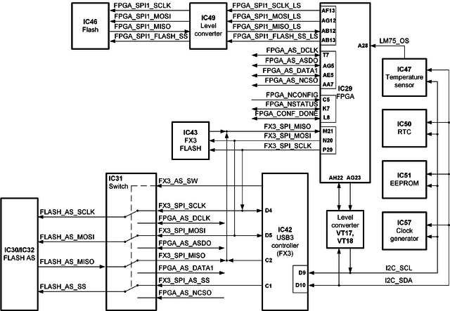
LimeSDR-QPCIe board low speed interface is divided into FPGA-RF and FPGA-FX3 groups and are presented in Figure 6 and Figure 7. The latter block diagrams depict the main ICs, corresponding IC pin numbers, data buses and serial protocol addresses.
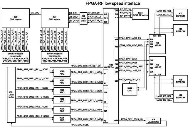
LimeSDR-QPCIe board peripherals can be controlled via USB interface. All commands that comes from USB are firstly processed by FX3 controller. I2C and multiple SPI interfaces provide connection to various on-board ICs, such as temperature sensor, port expander, clock generator, memory and real-time clock (RTC).
SPI interfaces
There are several SPI interfaces with their slave devices:
- FX3_SPI - Master of this bus is CYUSB3013 (IC42) and this bus has these slave devices:
- Flash memory M25P40 (IC43) dedicated for FX3 firmware;
- Flash memory W25Q128 (IC30) or S25FL128 (IC32) dedicated for FPGA configuration file. Using switch (IC31) flash memory is switched from FPGA to FX3_SPI BUS. Then flash content is updated and flash memory is switched back to FPGA. This is done when it is needed to update FPGA gateware in flash memory.
- FPGA (IC29) - If SPI slave is implemented in FPGA logic it can be accessed through FX3_SPI interface.
| FX3 pin (IC42) | FX3 chip reference (IC42) | FX3 pin (IC42) | FPGA pin (IC29) | I/O standard |
|---|---|---|---|---|
| D4 | SPI_SCK | FX3_SPI_SCLK | P20 | 3.3V |
| D5 | SPI_MOSI | FX3_SPI_MOSI | N20 | 3.3V |
| C2 | SPI_MISO | FX3_SPI_MISO | M21 | 3.3V |
| F5 | GPIO[46] | FX3_SPI_FPGA_SS | AG22 | 3.3V |
| F2 | GPIO[45] | FX3_SPI_AS_SS | - | 3.3V |
| C1 | SPI_SSN | FX3_SPI_FLASH_SS | - | 3.3V |
- FPGA_SPI0 – master of this interface is FPGA (IC29), slave devices of this interface:
- RFIC LMS7002M (IC1)
- RFIC LMS7002M (IC2)
- 14-bit ADC ADS4246 (IC37)
- XO VC DAC AD5662 (IC54)
- Phase detector ADF4002 (IC53)
| Schematic signal name | FPGA pin(IC29) | I/O standard | Comment |
|---|---|---|---|
| FPGA_SPI0_SCLK | T25 | 2.5V(3.3V) | |
| FPGA_SPI0_MOSI | R26 | 2.5V(3.3V) | |
| FPGA_SPI0_MISO_LMS1 | R30 | 2.5V(3.3V) | |
| FPGA_SPI0_MISO_LMS2 | V30 | 2.5V(3.3V) | |
| FPGA_SPI0_MISO_ADC | L20 | 1.8V | |
| FPGA_SPI0_LMS1_SS | V29 | 2.5V(3.3V) | |
| FPGA_SPI0_LMS2_SS | U29 | 2.5V(3.3V) | |
| FPGA_SPI0_ADC_SS | E26 | 1.5V | Configure FPGA output as Open-Drain |
| FPGA_SPI0_DAC_SS | G23 | 1.5V | Configure FPGA output as Open-Drain |
| FPGA_SPI0_ADF_SS | E25 | 1.5V | Configure FPGA output as Open-Drain |
- FPGA_SPI1: master of this interface is FPGA (IC29), slave devices of this interface:
- Flash memory M25P40 (IC46)
| Schematic signal name | FPGA pin(IC29) | I/O standard | Comment |
|---|---|---|---|
| FPGA_SPI1_SCLK_LS | AF13 | 1.5V | Connected through voltage level shifter. Net label on memory side FPGA_SPI1_SCLK |
| FPGA_SPI1_MOSI_LS | AG12 | 1.5V | Connected through voltage level shifter. Net label on memory side FPGA_SPI1_MOSI |
| FPGA_SPI1_MISO_LS | AB12 | 1.5V | Connected through voltage level shifter. Net label on memory side FPGA_SPI1_MISO |
| FPGA_SPI1_FLASH_SS_LS | AB13 | 1.5V | Connected through voltage level shifter. Net label on memory side FPGA_SPI1_FLASH_SS |
- FPGA_SPI2: master of this interface is FPGA (IC29), slave devices of this interface:
- 6x ADC (IC18, IC20, IC23, IC25, IC26, IC28) dedicated for onboard RSSI use.
| Schematic signal name | FPGA pin(IC29) | I/O standard | Comment |
|---|---|---|---|
| FPGA_SPI2_SCLK_LS | AK15 | 1.5V | Connected through voltage level shifter and clock buffer to all six ADC. Net label after level shifter FPGA_SPI2_SCLK. Fanouts through clock buffer to nets:
FPGA_SPI2_LMS1_RX1_I_SCLK, FPGA_SPI2_LMS1_RX1_Q_SCLK, FPGA_SPI2_LMS2_RX2_I_SCLK, FPGA_SPI2_LMS2_RX1_Q_SCLK, FPGA_SPI2_LMS2_RX1_I_SCLK, FPGA_SPI2_LMS2_RX2_Q_SCLK |
| FPGA_SPI2_LMS1_RX1_I_MISO | J7 | 1.5V | |
| FPGA_SPI2_LMS1_RX1_Q_MISO | A3 | 1.5V | |
| FPGA_SPI2_LMS2_RX1_I_MISO | H15 | 1.5V | |
| FPGA_SPI2_LMS2_RX1_Q_MISO | G9 | 1.5V | |
| FPGA_SPI2_LMS2_RX2_I_MISO | C27 | 1.5V | |
| FPGA_SPI2_LMS2_RX2_Q_MISO | F6 | 1.5V | |
| FPGA_SPI2_LMS_RX_DET_SS | AJ17 | 1.5V |
I2C interfaces
Board has three independent I2C interfaces: I2C, LMS1_I2C and LMS2_I2C. I2C – master of this interface can be either FX3 (IC42) or either FPGA (IC29). Master selection is done through R287 and R288 resistors. By default, master is FX3 (resistors fitted). To select FPGA as master, remove R287 and R288 resistors. This interface has several slave devices which are listed in Table 23.
- RTC DS3231 (IC50);
- EEPROM M24128 (IC51);
- Temperature sensor LM75 (IC47), EEPROM and clock generator. Information for slave devices are provided in Table 23, signal connectivity information is in Table 24.
| I2C slave device | Slave device | I2C address | I/O standard | Comment |
|---|---|---|---|---|
| IC47 | Temperature sensor | 1 0 0 1 0 0 0 RW | 3.3V | LM75 |
| IC51 | EEPROM | 1 0 1 0 0 0 0 RW | 3.3V | M24128 |
| IC57 | Clock generator | 1 1 0 0 0 0 0 RW | 3.3V | Si5351C |
| IC50 | Real-time clock (RTC) | 1 1 0 1 0 0 0 RW | 3.3V | DS3231 |
| Schematic signal name | FPGA pin (IC29) | FX3 pin (IC42) | I/O standard | Comment |
|---|---|---|---|---|
| I2C_SDA_LS | AH22 | - | 1.5V | Connected through level converter to I2C_SDA. Remove R287 and R288 to use FPGA as I2C master. |
| I2C_SCL_LS | AG23 | - | 1.5V | Connected through level converter to I2C_SCL. Remove R287 and R288 to use FPGA as I2C master. |
| FX3_I2C_SDA | - | D9 | 3.3V | Connected through R287 to I2C_SDA. |
| FX3_I2C_SCL | - | D10 | 3.3V | Connected through R288 to I2C_SCL. |
- LMS1_I2C: this interface has two EEPROMs. This interface is only accessible from LMS7002M (IC1). In Table 25 are listed all LMS1_I2C slave devices and their information. In Table 26 listed pin connections.
| I2C slave device | Slave device | I2C address | I/O standard | Comment |
|---|---|---|---|---|
| IC3 | EEPROM for LMS7 MCU firmware | 1 0 1 0 A2 A1 A0 RW | 2.5V(3.3V) | M24128 |
| IC4 | EEPROM | 1 0 1 0 A2 A1 A0 RW | 2.5V(3.3V) | 24FC512 |
| Schematic signal name | RFIC pin (IC1) | I/O standard | Comment |
|---|---|---|---|
| LMS1_I2C_SDA | D26 | 2.5V(3.3V) | Accessible only from IC1 |
| LMS1_I2C_SCL | C27 | 2.5V(3.3V) | Accessible only from IC1 |
- LMS2_I2C: this interface has two EEPROMs. This interface is only accessible from LMS7002M (IC2). In Table 27 are listed all LMS1_I2C slave devices and their information. In Table 28 listed pin connections.
| I2C slave device | Slave device | I2C address | I/O standard | Comment |
|---|---|---|---|---|
| IC5 | EEPROM for LMS7 MCU firmware | 1 0 1 0 A2 A1 A0 RW | 2.5V(3.3V) | M24128 |
| IC6 | EEPROM | 1 0 1 0 A2 A1 A0 RW | 2.5V(3.3V) | 24FC512 |
| Schematic signal name | RFIC pin (IC2) | I/O standard | Comment |
|---|---|---|---|
| LMS2_I2C_SDA | D26 | 2.5V(3.3V) | Accessible only from IC2 |
| LMS2_I2C_SCL | C27 | 2.5V(3.3V) | Accessible only from IC2 |
UART
UART interface is dedicated for communication between FPGA and GNSS receiver GPS/GNSS M0578 (IC48).
| Schematic signal name | FPGA pin (IC29) | I/O standard |
|---|---|---|
| GNSS_RX | K25 | 3.3V(2.5V) |
| GNSS_TX | K22 | 3.3V(2.5V) |
User I/O
This chapter describes available inputs and outputs of LimeSDR-QPCIe v1.2 board which can be used for user applications.
FPGA switch
4 poles slide switch SW2 is connected to FPGA and can be used to implement additional functionality which requires input control. Each switch line has external pull up resistors. When switch is in position “On”, it pulls down the line to logic ‘0’ level.
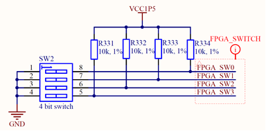
In Table 30 are listed each switch line and correspond FPGA pins.
| Switch pole | Schematic signal name | FPGA pin(IC29) | I/O standard |
|---|---|---|---|
| 1 | FPGA_SW0 | H7 | 1.5V |
| 2 | FPGA_SW1 | A2 | 1.5V |
| 3 | FPGA_SW2 | E6 | 1.5V |
| 4 | FPGA_SW3 | F8 | 1.5V |
Indication LEDs
LimeSDR-QPCIe board comes with four single colour (green) general purpose LEDs, one general purpose dual colour (red-green) LED, one green LED informing about successful FPGA configuration and one for power indication.
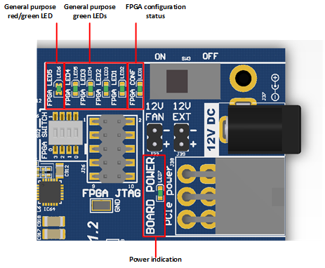
All LEDs are connected to FPGA and their function can be changed except for LED1. Default LEDs functions and other information are listed in the table below.
| Board Reference | Schematic name | Board label | Type | Description |
|---|---|---|---|---|
| LED1 | FPGA_CONF_DONE | FPGA CONF | FPGA status | LED lights up after successful FPGA configuration |
| LED2, LED3, LED4, LED5 | FPGA_LED1, FPGA_LED2, FPGA_LED3, FPGA_LED4 | FPGA LED1, FPGA LED2, FPGA LED3, FPGA LED4 | General purpose | General purpose reconfigurable single colour LED. |
| LED6 | FPGA_LED5_G, FPGA_LED5_R | FPGA LED5 | General purpose | General purpose reconfigurable dual colour (red-green) LED. |
| LED7 | VCC3P3, GND | BOARD POWER | Power indication | LED lights up when VCC3P3 power rail is active. |
RF Loopback Control
There is RF loopback circuit for RF transceivers which can be controlled from FPGA through shift registers 74HC595 (IC7 and IC8). Pin connection can be found in Table 32.
| Schematic signal name | FPGA pin(IC29) | I/O standard | Comment |
|---|---|---|---|
| SR_SCLK_LS | AA13 | 1.5V | Connected through level converter to SR_SCLK. |
| SR_DIN_LS | AJ5 | 1.5V | Connected through level converter to SR_DIN. |
| SR_LATCH_LS | B26 | 1.5V | Connected through level converter to SR_LATCH. |
| IC7 pin reference | Result | |||||||
|---|---|---|---|---|---|---|---|---|
| Q0 | Q1 | Q2 | Q3 | Q4 | Q5 | Q6 | Q7 | |
| x | x | x | x | L | H | x | x | LMS#1 TX1_2 → U.FL (J13) |
| x | x | x | x | H | L | x | x | LMS#1 TX1_2 → LMS#1 RX1_H |
| x | x | H | x | x | x | x | x | LMS#1 TX1_2 shunt to ground on |
| x | x | L | x | x | x | x | x | LMS#1 TX1_2 shunt to ground off |
| x | x | x | H | x | x | x | x | LMS#1 TX1_2 → RX1_H attenuation -40 dB |
| x | x | x | L | x | x | x | x | LMS#1 TX1_2 → RX1_H attenuation -25 dB |
| x | x | x | x | x | x | L | H | LMS#1 TX2_2 → U.FL (J17) |
| x | x | x | x | x | x | H | L | LMS#1 TX2_2 → LMS#1 RX2_H |
| H | x | x | x | x | x | x | x | LMS#1 TX2_2 shunt to ground on |
| L | x | x | x | x | x | x | x | LMS#1 TX2_2 shunt to ground off |
| x | H | x | x | x | x | x | x | LMS#1 TX2_2 → RX2_H attenuation -40 dB |
| x | L | x | x | x | x | x | x | LMS#1 TX2_2 → RX2_H attenuation -25 dB |
Note 1: 	Schematic signals corresponds to IC7 pins as below:
Q0 – LMS1_TX2_2_LB_SH	Q1 – LMS1_TX2_2_LB_AT	Q2 – LMS1_TX1_2_LB_SH	Q3 – LMS1_TX1_2_LB_AT
Q4 – LMS1_TX1_2_LB_H	Q5 – LMS1_TX1_2_LB_L	Q6 – LMS1_TX2_2_LB_H	Q7 – LMS1_TX2_2_LB_L
| IC8 pin reference | Result | |||||||
|---|---|---|---|---|---|---|---|---|
| Q0 | Q1 | Q2 | Q3 | Q4 | Q5 | Q6 | Q7 | |
| x | x | H | L | x | x | x | x | LMS#2 TX1_2 → U.FL (J14) |
| x | x | L | H | x | x | x | x | LMS#2 TX1_2 → LMS#2 RX1_H |
| x | x | x | x | x | H | x | x | LMS#2 TX1_2 shunt to ground on |
| x | x | x | x | x | L | x | x | LMS#2 TX1_2 shunt to ground off |
| x | x | x | x | x | x | H | x | LMS#2 TX1_2 → RX1_H attenuation -40 dB |
| x | x | x | x | x | x | L | x | LMS#2 TX1_2 → RX1_H attenuation -25 dB |
| H | L | x | x | x | x | x | x | LMS#2 TX2_2 → U.FL (J18) |
| L | H | x | x | x | x | x | x | LMS#2 TX2_2 → LMS#2 RX2_H |
| x | x | x | x | x | x | x | H | LMS#2 TX2_2 shunt to ground on |
| x | x | x | x | x | x | x | L | LMS#2 TX2_2 shunt to ground off |
| x | x | x | x | H | x | x | x | LMS#2 TX2_2 → RX2_H attenuation -40 dB |
| x | x | x | x | L | x | x | x | LMS#2 TX2_2 → RX2_H attenuation -25 dB |
Note 1:
 Q0 – LMS2_TX2_2_LB_L	Q1 – LMS2_TX2_2_LB_H	Q2 – LMS2_TX1_2_LB_L	Q3 – LMS2_TX1_2_LB_H
 Q4 – LMS2_TX2_2_LB_AT	Q5 – LMS2_TX1_2_LB_SH	Q6 – LMS2_TX1_2_LB_AT	Q7 – LMS2_TX2_2_LB_SH
The table below describes RF transceiver LMS7002#1 and LMS7002#2 external loopback configuration, pins, schematic signal name, FPGA interconnections and I/O standard.
| Loopback for | RF switch | Schematic control signal name | Shift register pin | FPGA-shift register pins | Comment |
|---|---|---|---|---|---|
| LMS7002 #1 (IC1) | IC10, IC12 | LMS1_TX1_2_LB_L LMS1_TX1_2_LB_H | IC7.Q5 IC7.Q4 | AJ5, AA13, B26 (through level shifter IC9) | When LMS1_TX1_2_LB_L is high andLMS1_TX1_2_LB_H is low then LMS#1 TX1_2 (LMS1_LOOPBACK_TX12 net) is fed to U.FL connector J13. When LMS1_TX1_2_LB_L is low and LMS1_TX1_2_LB_H is high then LMS#1 TX1_2 (LMS1_LOOPBACK_TX12 net) is fed to LMS#1 RX1_H (LMS1_LOOPBACK_RX1H net) |
| IC14, IC15 | LMS1_TX2_2_LB_L LMS1_TX2_2_LB_H | IC7.Q7 IC7.Q6 | When LMS1_TX2_2_LB_L is high and LMS1_TX2_2_LB_H is low then LMS#1 TX2_2 (LMS1_LOOPBACK_TX22 net) is fed to U.FL connector J17. When LMS1_TX2_2_LB_L is low and LMS1_TX2_2_LB_H is high then LMS#1 TX2_2 (LMS1_LOOPBACK_TX22 net) is fed to LMS#1 RX2_H (LMS1_LOOPBACK_RX2H net) | ||
| VT3, VT9 | LMS1_TX1_2_LB_SH | IC7.Q2 | Loopback shunt to ground for high isolation. When high – shunt active, when low – shunt off. | ||
| VT1 | LMS1_TX1_2_LB_AT | IC7.Q0 | When LMS1_TX1_2_LB_AT is low, TX1_2 to RX1_H loopback attenuation is set to -40 dB. When LMS1_TX1_2_LB_AT is high, loopback attenuation is set to -25 dB. | ||
| VT7 | LMS1_TX2_2_LB_AT | IC7.Q1 | When LMS1_TX2_2_LB_AT is low, TX2_2 to RX2_H loopback attenuation is set to -40 dB. When LMS1_TX2_2_LB_AT is high, loopback attenuation is set to -25 dB. | ||
| LMS7002#2 (IC2) | IC11, IC13 | LMS2_TX1_2_LB_L LMS2_TX1_2_LB_H | IC8.Q2 IC8.Q3 | When LMS2_TX1_2_LB_L is high and LMS2_TX2_2_LB_H is low then LMS#2 TX1_2 (LMS2_LOOPBACK_TX12 net) is fed to U.FL connector J14. When LMS2_TX1_2_LB_L is low and LMS2_TX1_2_LB_H is high then LMS#2 TX1_2 (LMS2_LOOPBACK_TX12 net) is fed to LMS#2 RX1_H (LMS2_LOOPBACK_RX1H net) | |
| IC15, IC17 | LMS2_TX2_2_LB_L LMS2_TX2_2_LB_H | IC8.Q0 IC8.Q1 | When LMS2_TX2_2_LB_L is high and LMS2_TX2_2_LB_H is low then LMS#2 TX2_2 (LMS2_LOOPBACK_TX22 net) is fed to U.FL connector J18. When LMS2_TX2_2_LB_L is low and LMS2_TX2_2_LB_H is high then LMS#2 TX2_2 (LMS2_LOOPBACK_TX22 net) is fed to LMS#2 RX2_H (LMS2_LOOPBACK_RX2H net) | ||
| VT11, VT12 | LMS2_TX2_2_LB_SH | IC8.Q7 | Loopback shunt to ground for high isolation. When high – shunt active, when low – shunt off. | ||
| VT2 | LMS2_TX1_2_LB_AT | IC8.Q6 | When LMS2_TX1_2_LB_AT is low, TX1_2 to RX1_H loopback attenuation is set to -40 dB. When LMS2_TX1_2_LB_AT is high, loopback attenuation is set to -25 dB. | ||
| VT8 | LMS2_TX2_2_LB_AT | IC8.Q4 | When LMS2_TX2_2_LB_AT is low, TX2_2 to RX2_H loopback attenuation is set to -40 dB. When LMS2_TX2_2_LB_AT is high, loopback attenuation is set to -25 dB. |
Board Temperature Control
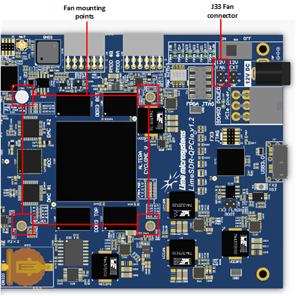
LimeSDR-QPCIe has integrated temperature sensor (IC47) which controls FAN to keep board in operating temperature range. FAN has dedicated holes for mounting over the main digital ICs (FPGA, DDRs, DACs and ADC) and must be connected to J33 (0.1” pitch) connector. Fan will be turned on when board heats up to 55°C and will be turned off when the temperature reduces to 45°C.
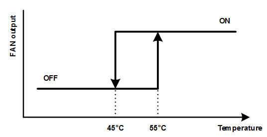
Measured temperature value can read by using LimeSuiteGUI as described in chapter “3.13 Reading Board Temperature”.
LimeSDR-QPCIe board comes with a dedicated 60mm DC FAN mounting space. Three M3 exposed copper holes (connected to board GND plane) and a space for a standoff are provided and are shown in Figure 11. The hole centre to hole centre distance is 50mm.The FAN is controlled via J33 (0.1” pitch) connector which can provide either 12V (default) or a 5V supply rail. The gate of the FAN driving MOSFET is connected to IC29 (FPGA) pin J22 (2.5V/3.3V bank).
Clock Distribution
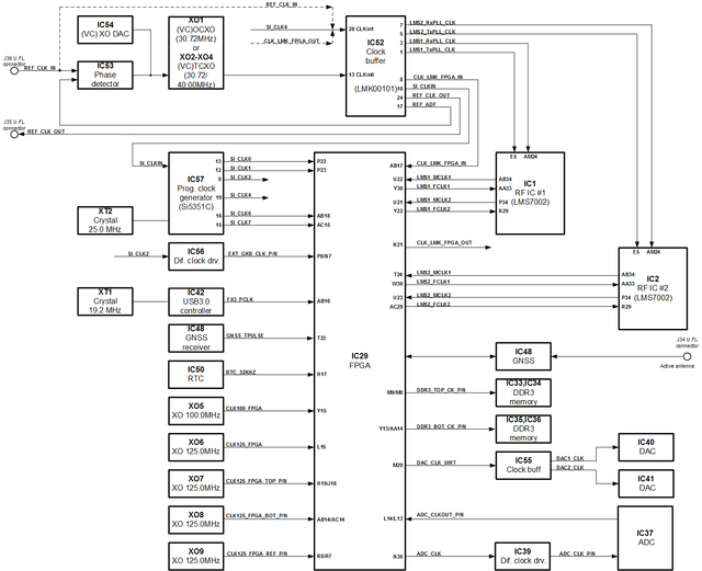
LimeSDR-QPCIe board clock distribution block diagram is presented in Figure 12.
Main clock sources
There are various crystal oscillators with various frequencies mounted on LimeSDR-QPCIe board. The programmable clock generator IC37 (Si5351C [link]) can generate any reference clock frequency, starting from 8 kHz – 160 MHz, for FPGA and LMS PLLs. A real-time clock (RTC) chip (IC50) is also included on the LimeSDR-QPCIe board. The output of IC50 is connected to the FPGA pin H17. Main clock sources and destinations are listed in Table 36.
| Src. | Dest. | Schematic net name | Freq. | I/O standard | FPGA pin | Description |
|---|---|---|---|---|---|---|
| Clk. Gen. (IC57) | FPGA | SI_CLK0 | 8kHz-160MHz | 2.5/3.3V | P22 | |
| SI_CLK1 | 8kHz-160MHz | 2.5/3.3V | P23 | |||
| EXT_GXB_CLK_P | 8kHz-160MHz | LVDS | P8 | Single-ended converted to differential through IC56 | ||
| EXT_GXB_CLK_N | N7 | |||||
| Clk. Buff. (IC52) | SI_CLK4 | 8kHz-160MHz | - | - | Can be selected as IC52 CLKin1 clock source | |
| FPGA | SI_CLK6 | 8kHz-160MHz | 1.5V | AB18 | ||
| SI_CLK7 | 1.5V | AC15 | ||||
| FX3 (IC42) | FPGA | FX3_PCLK | 66MHz, 100MHz | 1.5V | AB16 | |
| GNSS (IC48) | FPGA | GNSS_TPULSE | * | 3.3V/2.5V | T23 | |
| RTC (IC50) | FPGA | RTC_32KHZ | 32kHz | 1.5V | H17 | |
| XO5 | FPGA | CLK100_FPGA | 100MHz | 1.5V | Y15 | |
| XO6 | FPGA | CLK125_FPGA | 125MHz | 1.5V | L15 | |
| XO7 | FPGA | CLK125_FPGA_TOP_P | 125MHz | LVDS | H19 | |
| CLK125_FPGA_TOP_N | J18 | |||||
| XO8 | FPGA | CLK125_FPGA_BOT_P | 125MHz | LVDS | AB14 | |
| CLK125_FPGA_BOT_N | AC14 | |||||
| XO9 | FPGA | CLK125_FPGA_REF_P | 125MHz | LVDS | R8 | |
| CLK125_FPGA_REF_N | R7 | |||||
| FPGA | DAC (IC40, IC41) | DAC_CLK_WRT | * | 2.5/3.3V | M29 | Goes through clock buffer (IC21) |
| Clk. Buff. (IC52) | FPGA | CLK_LMK_FPGA_IN | * | 1.5V | AB17 | |
| RFIC (IC1) | FPGA | LMS1_MCLK1 | * | 2.5/3.3V | U22 | |
| LMS1_MCLK2 | * | 2.5/3.3V | U21 | |||
| FPGA | RFIC (IC1) | LMS1_FCLK1 | * | 2.5/3.3V | Y30 | |
| LMS1_FCLK2 | * | 2.5/3.3V | Y22 | |||
| FPGA | Clk. Buff. (IC52) | LMK_CLK_FPGA_OUT | * | 2.5/3.3V | N21 | |
| RFIC (IC2) | FPGA | LMS2_MCLK1 | * | 2.5/3.3V | T24 | |
| LMS2_MCLK2 | * | 2.5/3.3V | U23 | |||
| FPGA | RFIC (IC2) | LMS2_FCLK1 | * | 2.5/3.3V | W30 | |
| LMS2_FCLK2 | * | 2.5/3.3V | AC29 | |||
| FPGA | DDR3 (IC33, IC34) | DDR3_TOP_CK_P | * | Differential 1.5-V SSTL Class I | M9 | |
| DDR3_TOP_CK_N | * | M8 | ||||
| FPGA | DDR3 (IC35, IC36) | DDR3_BOT_CK_P | * | Differential 1.5-V SSTL Class I | Y13 | |
| DDR3_BOT_CK_N | * | AA14 | ||||
| FPGA | DAC (IC40, IC41) | DAC_CLK_WRT | * | 3.3V | M29 | Feeds both DAC through clock buffer (IC55) |
| ADC (IC37) | FPGA | ADC_CLKOUT_P | * | LVDS | L14 | |
| ADC_CLKOUT_N | * | L13 | ||||
| FPGA | ADC (IC37) | ADC_CLK | * | 3.3/2.5V | N30 | Converted from single ended to LVDS through IC39 |
Clock buffer source selection
Clock buffer (IC52) presented in Figure 12 provides clock signals for following components:
- LMS7002 transceivers (IC1, IC2);
- FPGA (IC29) pin AB17;
- Phase detector (IC53);
- Clock generator (IC57);
- U.FL connector J35 (REF CLK OUT label on board). To use this output 0R resistor R378 has to be fitted.
CLKin0 – to select this input as a source for Clock buffer (IC52) R375 resistor has to be removed (removed by default). As a source for this input one of the following high-precision crystal oscillators can be selected:
- XO1 – 30.72 MHz VCOCXO (precision: ±20 ppb stable);
- XO2 or XO3 – 30.72 MHz VCTCXO (precision: ±1 ppm initial, ±4 ppm stable);
- XO4 – 40 MHz VCTCXO (precision: ±1 ppm initial).
IC52 buffer CLKin0 clock source is selected by one of the 0402 size 0R resistor combinations, required modifications can be found in Table 37.
| Source for clock buffer (IC52) CLKin0 input | 0R Fit | 0R NF | Comment |
|---|---|---|---|
| XO1 | R364, R365 | R379, R380, R382, R384 | Default selection |
| XO2, X03 | R379, R380 | R364, R365, R382, R384 | |
| XO4 | R382, R384 | R364, R365, R379, R380 |
CLKin1 – to select this input as a source for Clock buffer (IC52) R375 resistor has to be fitted (removed by default). As a source for this input one of the following sources can be selected:
- Clock generator (IC57)
- U.FL Connector (J36)
- FPGA (IC29) output pin N21
| Source for clock buffer (IC52) CLKin1 input | Schematic net name | 0R Fit | 0R NF | Comment |
|---|---|---|---|---|
| Clock generator (IC57) output CLK4 | SI_CLK4 | R374 | R368, R372 | Default selection |
| J36 U.FL Connector | REF_CLK_IN | R372 | R368, R374, R389 | |
| FPGA (IC29) output pin N21 | CLK_LMK_FPGA_OUT | R368 | R372, R374 |
VCTCXO clock tuning
VCTCXO can be tuned by on-board phase detector (IC53, ADF4002 [[2]]) or by 16-bit DAC (IC54). The on-board phase detector is used to synchronize on-board VCTCXO with external equipment (via J36 U.FL connector) to calibrate frequency error. At the same time only ADF or DAC can control VCTCXO. Both ADF and DAC are connected to FPGA_SPI0 interface. For details see chapter SPI interfaces. With valid configuration selection between ADF and DAC is done automatically. When board is powered, by default VCTCXO is controlled by DAC.
Power Distribution
LimeSDR-QPCIe board can be powered from several sources. The first power supply source option is 12V DC through a 2.5mm centre positive barrel connector. The second one is through a standard 6-pin PCIe power connector J38 (0.165” pitch). The last supply source option is the board edge PCIe connector.
LimeSDR-QPCIe board has complex power delivery network consisting of many different power rails with different voltages, filters, power sequences. LimeSDR-QPCIe board power distribution block diagram is presented in Figure 13 in two parts.
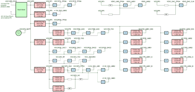
Power network power circuit ICs are presented in Figure 14 and Figure 15.
