DE0-Nano Interface Board: Difference between revisions
Ghalfacree (talk | contribs) (Initial page creation.) |
Ghalfacree (talk | contribs) (Added schematics as a gallery.) |
||
| Line 13: | Line 13: | ||
===Schematics=== | ===Schematics=== | ||
<gallery> | |||
File:DE0-Nano-Interface-Board-Schematics-1.png|Data interface connector | |||
File:DE0-Nano-Interface-Board-Schematics-2.png|FPGA module | |||
File:DE0-Nano-Interface-Board-Schematics-3.png|Hi-Speed USB 2.0 interface | |||
File:DE0-Nano-Interface-Board-Schematics-4.png|Clock generator | |||
File:DE0-Nano-Interface-Board-Schematics-5.png|Power supply for clock generator | |||
File:DE0-Nano-Interface-Board-Schematics-6.png|I²C port expander | |||
</gallery> | |||
===See Also=== | ===See Also=== | ||
Revision as of 14:45, 16 July 2015
About
The DE0-Nano Interface Board, also known as the Digital Interface Board, allows the Myriad-RF 1 to be paired with the DE0-Nano FPGA Development System through the RFDIO Interface. The DE0-Nano Interface Board acts as a motherboard for the Myriad-RF 1 and the DE0-Nano FPGA Development System, mating the two together with a high-speed interface. The DE0-Nano Interface Board is not designed for use with any other FPGA development system; for other development systems, the Zipper Interface Board should be used instead.
Images
-
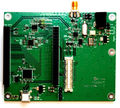
DE0-Nano Interface Board, top
-
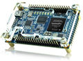
DE0-Nano FPGA Development System
-
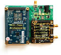
DE0-Nano Interface Board with DE0-Nano and Myriad-RF 1


Connections
The DE0-Nano Interface Board features numerous on-board connections, in addition to those available on the Myriad-RF 1 and DE0-Nano themselves. A full list of available connections is available on the page DE0-Nano Interface Board Connections.
Schematics
-

Data interface connector
-

FPGA module
-

Hi-Speed USB 2.0 interface
-

Clock generator
-

Power supply for clock generator
-

I²C port expander


