LimeSDR-Mini v1.1 hardware description
LimeSDR-Mini Board Key Features
The LimeSDR-Mini is low-cost software defined radio board. LimeSDR-Mini development board provides a hardware platform for developing and prototyping high-performance and logic-intensive digital and RF designs using Intel’s MAX 10 FPGA and Lime Microsystems transceiver.
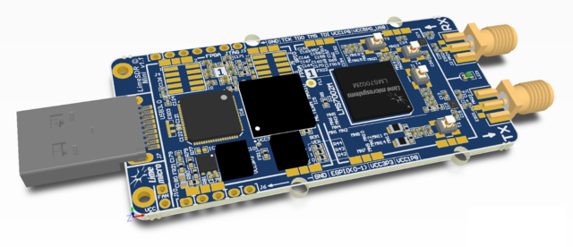
LimeSDR-Mini board features:
- USB 3.0 controller: FTDI FT601
- FPGA: Intel MAX 10 (10M16SAU169C8G 169-UBGA)
- 169-pin FBGA package
- 16 K LE
- 549 Kb M9K Memory
- 2368 Kb User Flash Memory
- 1x fractional phase locked loops (PLLs)
- 45x 18x18-bit multipliers
- 130x general purpose input/output (GPIO)
- Single supply
- Flash feature
- FPGA configuration via JTAG
- RF transceiver: Lime Microsystems LMS7002M
- EEPROM Memory: 2x 128Kb EEPROMs for LMS MCU firmware and FPGA data
- FLASH Memory: 4Mb Flash memory for FPGA data
- Temperature sensor (unpopulated)
- General user inputs/outputs:
- 1x Dual colour (RG) LED
- 8x + 2x FPGA GPIO pinheader (3.3V)
- Connections:
- USB3.0 (type A) plug
- Coaxial RF (SMA female) connectors
- FPGA GPIO headers (unpopulated)
- FPGA JTAG connector (unpopulated)
- FAN (5V or 3.3V) connector
- Clock system:
- 40.00MHz onboard VCTCXO
- Possibility to tune VCTCXO by onboard DAC
- Reference clock input and output connectors (U.FL)
- Board size: 69mm x 31.4mm
For more information on the following topics, refer to the respective documents:
- FTDI FT601 USB 3.0 to FIFO Bridge datasheet [link]
- MAX 10 FPGA device family, refer to MAX 10 Device Handbook [link]
- LMS7002M transceiver resources [link]
Board Overview
This section contains component location description on the board. LimeSDR-Mini board picture with highlighted connectors and main components is presented in Figure 2 and Figure 3.
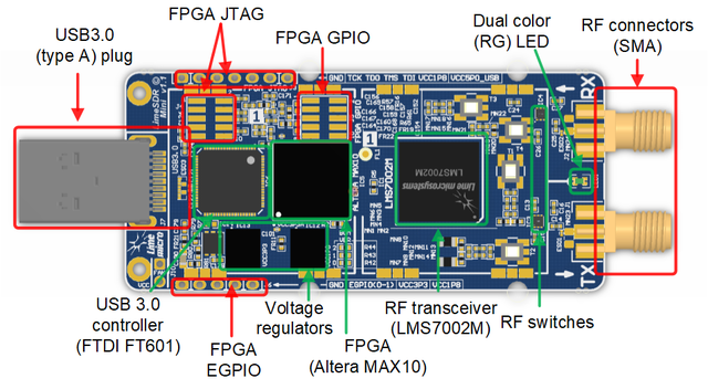
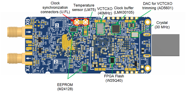
Board components description listed in the Table 1.
| Featured Devices | ||
|---|---|---|
| Board reference | Type | Description |
| IC1 | FPRF | Field programmable RF transceiver, LMS7002M |
| IC5 | FPGA | Intel MAX 10 (10M16SAU169C8G 169-UBGA) |
| IC6 | USB 3.0 microcontroller | FTDI USB 3.0 to FIFO interface bridge chip FT601 |
| Miscellaneous devices onboard | ||
| IC8 | IC | Temperature sensor, LM75 |
| Configuration, Status and Setup Components | ||
| J3 | JTAG chain connector | FPGA programming pin header on the board edge for Altera USB-Blaster download cable, 0.1” pitch |
| J4 | JTAG chain connector | FPGA programming pin header for Altera USB-Blaster download cable, 0.05” pitch |
| LED1 or LED2 | LED1 or LED2c | USB3.0 microcontroller (IC13) boot configuration (PMODE0[2:0]) resistors. Default mode: SPI boot, On Failure - USB Boot |
| General User Input/Output | ||
| J5 | Pin header | 8x FPGA GPIOs, 3.3V, 0.05” pitch |
| J6 | Pin header | 2x FPGA GPIOs on the board edge, 3.3V, 0.1” pitch |
| J10 | Pin header | 5V (3.3V voltage can be chosen by resistors) fan connection pin headers, 0.1” pitch |
| Memory Devices | ||
| IC2 | IC | I²C EEPROM Memory 128Kb (16K x 8), connected to RF transceiver I2C bus |
| IC10 | IC | I²C EEPROM Memory 128Kb (16K x 8), connected to FPGA I2C bus |
| IC11 | IC11 | Quad SPI Flash Memory 4Mb (512K x 8), connected to FPGA SPI |
| Communication Ports | ||
| J7 | USB3.0 connector | USB3.0 connector |
| Clock Circuitry | ||
| XO1 | VCTCXO | 40.00 MHz Voltage Controlled Temperature Compensated Crystal Oscillatorc |
| IC9 | IC | DAC for TCXO (XT4) frequency tuning |
| IC7 | IC7 | Clock buffer |
| J8 | U.FL connector | Reference clock input |
| J9 | U.FL connector | Reference clock output |
| Reference clock output | ||
| IC12 | IC | Switching regulator (1.8V) |
| IC13 | IC | Switching regulator (3.3V) |
| IC14 | IC | Linear regulator (2.5V) |
RF Frequency Range
LimeSDR-Mini board covers RF frequency range from 10MHz up to 3.5GHz. There are different matching networks connected to the RF transceiver RF inputs and outputs (antennas):
- Use TX1_1 RF output for 2GHz - 3.5GHz frequency range
- Use TX1_2 RF output for 10MHz - 2GHz frequency range
- Use RX1_H RF input for 2GHz - 3.5GHz frequency range
- Use RX1_W RF input for 10MHz - 2GHz frequency range
LimeSDR-Mini Board Architecture
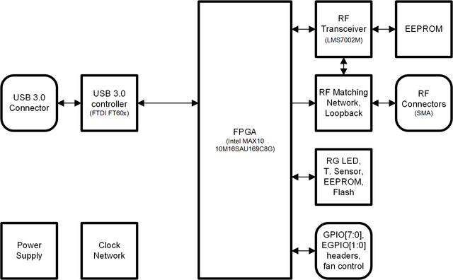
The heart of the LimeSDR-Mini board is Intel MAX 10 (10M16SAU169C8G 169-UBGA) FPGA. It’s main function is to transfer digital data between the PC through a USB3.0 connector. The block diagram for LimeSDR-Mini board is presented in the Figure 4.
LMS7002M Based Connectivity
The interface and control signals are described below:
- Digital Interface Signals: LMS7002 is using data bus LMS_DIQ1_D[11:0] and LMS_DIQ2_D[11:0], LMS_ENABLE_IQSEL1 and LMS_ENABLE_IQSEL2, LMS_FCLK1 and LMS_FCLK2, LMS_MCLK1 and LMS_MCLK2 signals to transfer data to/from FPGA. Indexes 1 and 2 indicate transceiver digital data PORT-1 or PORT-2. Any of these ports can be used to transmit or receive data. By default PORT-1 is selected as transmit port and PORT-2 is selected as receiver port. The FCLK# is input clock and MCLK# is output clock for LMS7002M transceiver. TXNRX signals sets ports directions. For LMS7002M interface timing details refer to LMS7002M transceiver datasheet page 12-13. [link].
- LMS Control Signals: these signals are used for optional functionality:
- LMS_RXEN, LMS_TXEN – receiver and transmitter enable/disable signals connected to FPGA Bank 8 (VDIO_LMS_FPGA; 2.5V).
- LMS_RESET – LMS7002M reset connected to FPGA Bank 7 (VDIO_LMS_FPGA; 2.5V).
- SPI Interface: LMS7002M transceiver is configured via 4-wire SPI interface; FPGA_SPI_SCLK, FPGA_SPI_MOSI, FPGA_SPI_MISO, FPGA_SPI_LMS_SS. The SPI interface controlled from FPGA Bank 2 (VDIO_LMS_FPGA; 2.5V).
- LMS I2C Interface: can be used for LMS EEPROM content modifying or for debug purposes. The signals LMS_I2C_SCL, LMS_I2C_DATA connected to FPGA Bank 2 (VDIO_LMS_FPGA; 2.5V).
| Chip pin (IC1) | Chip reference (IC1) | Schematic signal name | FPGA pin | FPGA I/O standard | Comment |
|---|---|---|---|---|---|
| E5 | xoscin_tx | TxPLL_CLK | - | 1.8V | Connected to 40.00 MHz clock |
| AB34 | MCLK1 | LMS_MCLK1 | G5 | 2.5V | |
| AA33 | FCLK1 | LMS_FCLK1 | L3 | 2.5V | |
| V32 | TXNRX1 | LMS_TXNRX1 | J8 | 2.5V | |
| U29 | TXEN | LMS_TXEN | K6 | 2.5V | |
| 1Y32 | ENABLE_IQSEL1 | LMS_ENABLE_IQSEL1 | M8 | 2.5V | |
| AG31 | DIQ1_D0 | LMS_DIQ1_D0 | M12 | 2.5V | |
| AF30 | DIQ1_D1 | LMS_DIQ1_D1 | N12 | 2.5V | |
| AF34 | DIQ1_D2 | LMS_DIQ1_D2 | N10 | 2.5V | |
| AE31 | DIQ1_D3 | LMS_DIQ1_D3 | L10 | 2.5V | |
| AD30 | DIQ1_D4 | LMS_DIQ1_D4 | M10 | 2.5V | |
| AC29 | DIQ1_D5 | LMS_DIQ1_D5 | M13 | 2.5V | |
| AE33 | DIQ1_D6 | LMS_DIQ1_D6 | N9 | 2.5V | |
| AD32 | DIQ1_D7 | LMS_DIQ1_D7 | N8 | 2.5V | |
| AC31 | DIQ1_D8 | LMS_DIQ1_D8 | M7 | 2.5V | |
| AC33 | DIQ1_D9 | LMS_DIQ1_D9 | N7 | 2.5V | |
| AB30 | DIQ1_D10 | LMS_DIQ1_D10 | M9 | 2.5V | |
| AB32 | DIQ1_D11 | LMS_DIQ1_D11 | N6 | 2.5V | |
| AM24 | xoscin_rx | RxPLL_CLK | - | 1.8V | Connected to 40.00 MHz clock |
| P34 | MCLK2 | LMS_MCLK2 | H4 | 2.5V | |
| R29 | FCLK2 | LMS_FCLK2 | M3 | 2.5V | |
| U31 | TXNRX2 | LMS_TXNRX2 | H5 | 2.5V | |
| V34 | RXEN | LMS_RXEN | M11 | 2.5V | |
| R33 | ENABLE_IQSEL2 | LMS_ENABLE_IQSEL2 | N3 | 2.5V | |
| H30 | DIQ2_D0 | LMS_DIQ2_D0 | M2 | 2.5V | |
| J31 | DIQ2_D1 | LMS_DIQ2_D1 | M4 | 2.5V | |
| K30 | DIQ2_D2 | LMS_DIQ2_D2 | M1 | 2.5V | |
| K32 | DIQ2_D3 | LMS_DIQ2_D3 | J1 | 2.5V | |
| L31 | DIQ2_D4 | LMS_DIQ2_D4 | N2 | 2.5V | |
| K34 | DIQ2_D5 | LMS_DIQ2_D5 | K1 | 2.5V | |
| M30 | DIQ2_D6 | LMS_DIQ2_D6 | L2 | 2.5V | |
| M32 | DIQ2_D7 | LMS_DIQ2_D7 | J2 | 2.5V | |
| N31 | DIQ2_D8 | LMS_DIQ2_D8 | N4 | 2.5V | |
| N33 | DIQ2_D9 | LMS_DIQ2_D9 | K2 | 2.5V | |
| P30 | DIQ2_D10 | LMS_DIQ2_D10 | L5 | 2.5V | |
| P32 | DIQ2_D11 | LMS_DIQ2_D11 | L4 | 2.5V | |
| U33 | CORE_LDO_EN | LMS_CORE_LDO_EN | N11 | 2.5V | |
| E27 | RESET | LMS_RESET | L1 | 2.5V | |
| D28 | SEN | FPGA_SPI_LMS_SS | J5 | 2.5V | SPI interface |
| C29 | SCLK | FPGA_SPI_SCLK | K5 | 2.5V | SPI interface |
| F30 | SDIO | FPGA_SPI_MOSI | J7 | 2.5V | SPI interface |
| F28 | SDO | FPGA_SPI_MISO | J6 | 2.5V | SPI interface |
| D26 | SDA | LMS_I2C_SDA | N5 | 2.5V | Connected to EEPROM |
| C27 | SCL | LMS_I2C_SCL | M5 | 2.5V | Connected to EEPROM |
USB 3.0 controller
Software controls LimeSDR-Mini board via the USB3 microcontroller (FTDI USB 3.0 to FIFO interface bridge chip FT601 [link]). The controller signals description showed below:
- FT_D[31:0] – FTDI 32-bit data interface is connected to FPGA.
- FT_TXEn, FT_RXFn, FT_SIWUn, FT_WRn, FT_RDn, FT_OEn, FT_BE[3:0] – FTDI interface control signals.
- FT_CLK – FTDI interface clock. Clock from FTDI is fed to FPGA.
In the table below are listed USB3.0 controller (FTDI) pins, schematic signal name, FPGA interconnections and I/O standard.
| Chip pin (IC6) | Chip reference (IC6) | Schematic signal name | FPGA pin | I/O standard | I/O standard |
|---|---|---|---|---|---|
| 40 | DATA_0 | FT_D0 | A2 | 3.3V | |
| 41 | DATA_1 | FT_D1 | B6 | 3.3V | |
| 42 | DATA_2 | FT_D2 | B3 | 3.3V | |
| 43 | DATA_3 | FT_D3 | B5 | 3.3V | |
| 44 | DATA_4 | FT_D4 | A3 | 3.3V | |
| 45 | DATA_5 | FT_D5 | B4 | 3.3V | |
| 46 | DATA_6 | FT_D6 | E6 | 3.3V | |
| 47 | DATA_7 | FT_D7 | A4 | 3.3V | |
| 50 | DATA_8 | FT_D8 | B12 | 3.3V | |
| 51 | DATA_9 | FT_D9 | H8 | 3.3V | |
| 52 | DATA_10 | FT_D10 | E9 | 3.3V | |
| 53 | DATA_11 | FT_D11 | B2 | 3.3V | |
| 54 | DATA_12 | FT_D12 | D9 | 3.3V | |
| 55 | DATA_13 | FT_D13 | J9 | 3.3V | |
| 56 | DATA_14 | FT_D14 | A9 | 3.3V | |
| 57 | DATA_15 | FT_D15 | H9 | 3.3V | |
| 60 | DATA_16 | FT_D16 | A7 | 3.3V | |
| 61 | DATA_17 | FT_D17 | F8 | 3.3V | |
| 62 | DATA_18 | FT_D18 | A6 | 3.3V | |
| 63 | DATA_19 | FT_D19 | E10 | 3.3V | |
| 64 | DATA_20 | FT_D20 | A5 | 3.3V | |
| 65 | DATA_21 | FT_D21 | F9 | 3.3V | |
| 66 | DATA_22 | FT_D22 | E8 | 3.3V | |
| 67 | DATA_23 | FT_D23 | A8 | 3.3V | |
| 69 | DATA_24 | FT_D24 | K11 | 3.3V | |
| 70 | DATA_25 | FT_D25 | K12 | 3.3V | |
| 71 | DATA_26 | FT_D26 | J12 | 3.3V | |
| 72 | DATA_27 | FT_D27 | G12 | 3.3V | |
| 73 | DATA_28 | FT_D28 | L13 | 3.3V | |
| 74 | DATA_29 | FT_D29 | G13 | 3.3V | |
| 75 | DATA_30 | FT_D30 | J13 | 3.3V | |
| 76 | DATA_31 | FT_D31 | H13 | 3.3V | |
| 58 | CLK | FT_CLK | G9 | 3.3V | |
| 4 | BE_0 | FT_BE0 | B11 | 3.3V | |
| 5 | BE_1 | FT_BE1 | C12 | 3.3V | |
| 6 | BE_2 | FT_BE2 | A12 | 3.3V | |
| 7 | BE_3 | FT_BE3 | B13 | 3.3V | |
| 8 | TXE_N | FT_TXEn | C13 | 3.3V | |
| 9 | RXF_N | FT_RXFn | A12 | 3.3V | |
| 10 | SIWU_N | FT_SIWUn | - | 3.3V | 10k pull up |
| 11 | WR_N | FT_WRn | E12 | 3.3V | |
| 12 | RD_N | FT_RDn | D12 | 3.3V | |
| 13 | OE_N | FT_OEn | F12 | 3.3V | |
| 15 | RESET_N | FT_RESETn | L12 | 3.3V | |
| 16 | WAKEP_N | FT_WAKEUPn | H10 | 3.3V |
Indication LEDs
LimeSDR-Mini board comes with one dual colour (red and green (RG)) indication LED. This LEDs can be soldered on the top (LED1) or on the bottom (LED2). By default, LED1 is populated and LED2 is unpopulated.
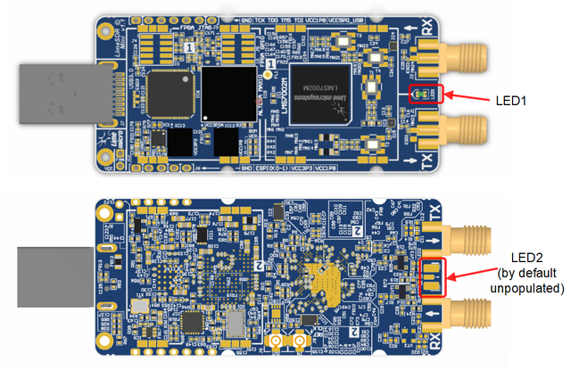
LEDs are connected to FPGA to the same lines and their function can be changed.
Low speed interfaces
LimeSDR-Mini board low speed interfaces are presented in Figure 6. The latter block diagrams depict the main ICs, corresponding IC pin numbers, data buses and serial protocol addresses.
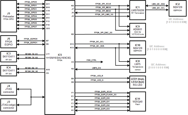
There are several SPI interfaces with their slave devices:
- FPGA_SPI: this SPI interface are connected to FPGA and slave devices can be accessed by transferring data to internal FPGA NIOS CPU. This bus has these slave devices RFIC (IC1) and DAC (IC9).
- FPGA_QSPI: this SPI interface is connected to Quad SPI flash memory (IC11).
- Internal FPGA SPI module: FPGA has its own SPI module and can be controlled as regular SPI device. By using FPGA SPI it is possible to control FPGA modes etc.
- FPGA_I2C: used to control external clock temperature sensor and EEPROM on LimeSDR-Mini board.
In the tables below are listed FPGA_SPI pins, schematic signal names, FPGA interconnections and I/O standards.
| Schematic signal name | FPGA pin | I/O standard | Comment |
|---|---|---|---|
| FPGA_SPI_SCLK | K5 | 2.5V (3.3V) | Serial Clock (FPGA output) |
| FPGA_SPI_MOSI | J7 | 2.5V (3.3V) | Data (FPGA output) |
| FPGA_SPI_MISO | J6 | 2.5V (3.3V) | Data (FPGA input) |
| FPGA_SPI_LMS_SS | J5 | 2.5V (3.3V) | IC1 (LMS7002) SPI slave select (FPGA output) |
| FPGA_SPI_DAC_SS | K8 | 2.5V (3.3V) | IC9 SPI slave select (FPGA output) |
In the tables below are listed FPGA_QSPI pins, schematic signal names, FPGA interconnections and I/O standards.
| Schematic signal name | FPGA pin | I/O standard | Comment |
|---|---|---|---|
| FPGA_QSPI_SCLK | F1 | 1.8V | Serial Clock (FPGA output) |
| FPGA_QSPI_IO0 | D1 | 1.8V | |
| FPGA_QSPI_IO1 | C1 | 1.8V | |
| FPGA_QSPI_IO2 | B1 | 1.8V | |
| FPGA_QSPI_FLASH_SS | E1 | 1.8V | FPGA_QSPI_FLASH_SS |
In the tables below are listed FPGA_I2C interface slave devices and their other information.
| I2C slave device | Slave device | I2C address | I/O standard | Comment |
|---|---|---|---|---|
| IC8 | Temperature sensor | 1 0 0 1 0 0 0 RW | 3.3V | LM75 |
| IC10 | EEPROM | 1 0 1 0 0 0 0 RW | 3.3V | M24128 |
8 GPIOs from FPGA are connected to 10 pin 0.05” header. Additional 2 pins are dedicated for power. Another 2 GPIOs are connected to 5 header on the board edge. In the tables below are listed FPGA_GPIO (J5) and FPGA_EGPIO (J6) information.
| Connector pin | Schematic signal name | FPGA pin | I/O standard | Comment |
|---|---|---|---|---|
| 1 | FPGA_GPIO0 | A11 | 3.3V | |
| 2 | FPGA_GPIO1 | B10 | 3.3V | |
| 3 | FPGA_GPIO2 | C10 | 3.3V | |
| 4 | FPGA_GPIO3 | D11 | 3.3V | |
| 5 | FPGA_GPIO4 | E13 | 3.3V | |
| 6 | FPGA_GPIO5 | F13 | 3.3V | |
| 7 | FPGA_GPIO6 | F10 | 3.3V | |
| 8 | FPGA_GPIO7 | G10 | 3.3V | |
| 9 | GND | - | Ground pin | |
| 10 | - | Selectable power net (3.3V or 5V). Default 3.3V |
| Connector pin | Schematic signal name | FPGA pin | I/O standard | Comment |
|---|---|---|---|---|
| 1 | GND | Ground pin | ||
| 2 | FPGA_EGPIO0 | B7 | 3.3V | |
| 3 | FPGA_EGPIO1 | D6 | 3.3V | |
| 4 | VCC3P3 | 3.3V | Power net (3.3V) | |
| 5 | VCC1P8 | 1.8V | Power net (1.8V) |
Board Temperature Control
LimeSDR-Mini has integrated temperature sensor which controls FAN to keep board in operating temperature range. FAN must be connected to J10 (0.1” pitch) connector. FAN control voltage is 5V, but it can be changed to 3.3V by resistors. Fan will be turned on if board will heat up to 55°C and FAN will be turned off if board will cool down to 45°C. By default temperature sensor is unpopulated and FAN is always on.
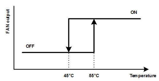
Clock Distribution
LimeSDR-Mini board clock distribution block diagram is presented in Figure 8. LimeSDR-Mini board has onboard 40.00 MHz VCTCXO that is reference clock for LMS and FPGA PLLs.
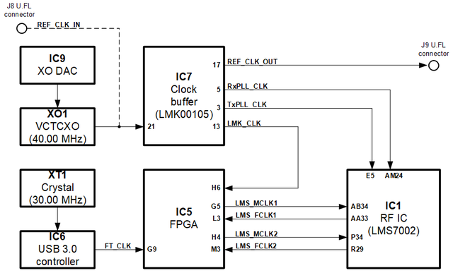
VCTCXO frequency can be tuned by using DAC (IC8). Buffered VCTCXO clock is connected to RF transceiver, FPGA. Buffered VCTCXO clock is also connected to connector J9 (REF_CLK_OUT) and can be fed to external hardware for synchronisation. VCTCXO can be disconnected from clock buffer input (remove R59 and solder R62) and external reference clock can be supplied from connector J8 (REF_CLK_IN).
| Source | Schematic net name | I/O standard | FPGA pin | Description |
|---|---|---|---|---|
| External | REF_CLK_IN | External reference clock input | ||
| Board | Board | 2.5V (3.3V) | Buffered reference clock output | |
| Clock buffer (IC7) | LMK_CLK | 2.5V (3.3V) | H6 | Buffered reference clock output |
| RF transceiver (IC1) | RxPLL_CLK | 2.5V (3.3V) | Buffered reference clock output | |
| TxPLL_CLK | 2.5V (3.3V) | Buffered reference clock output | ||
| LMS_MCLK1 | 2.5V (3.3V) | G5 | ||
| LMS_FCLK1 | 2.5V (3.3V) | L3 | ||
| LMS_MCLK2 | 2.5V (3.3V) | H4 | ||
| LMS_FCLK2 | 2.5V (3.3V) | M3 | ||
| USB3.0 controller | FT_CLK | 3.3V | G9 | 100 MHz |
External clock notes. External clock capabilities on LimeSDR-Mini board are defined by LMK00105 clock buffer specification. User must ensure voltage levels are in the range of LMK00105 capabilities. Ideally, a phase detector circuitry should be used to synchronize on board TCXO to the external clock but there simply is no space on LimeSDR-Mini for this functionality. Hence decision was made just to provide an input to LMK clock buffer for external clock connection. This means that user should pay attention on how external signal is connected, ensure proper voltage levels etc. If you supply external clock signal from signal generator, signal level should be around 10dBm. Note please, that LMK clock buffer expects positive voltage amplitude, while your generator may supply +/- voltage.
The proper way to supply the external reference clock: supply external clock firstfirst and then turn the board on. This is the only way to have proper operation of the board with external clock. If frequency is changed on the fly, CPU inside of FPGA gets messed up hence no control over the board.
Power Distribution
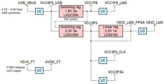
LimeSDR-Mini board is powered from USB port. LimeSDR-Mini board power delivery network consists of different power rails with different voltages, filters, power sequences. LimeSDR-Mini board power distribution block diagram is presented in Figure 9.
| |||||||||||||||||||||