LMS7002Mr3 Calibration Using MCU
Introduction
This page provides a brief description of the main calibration procedures used to improve the RF performance of LMS7002M IC by using the built-in microcontroller (MCU). It also contains information needed to program and run LMS7002M IC internal MCU, which handles the calibration procedure execution routines, thus greatly simplifying the calibration porting procedure to other systems.
General MCU calibration description
This section focuses on a brief description of the calibration procedures themselves that are handled by the program stored in MCU image. The calibration procedures for the LMS7002M chip are listed below:
- DC offset and LO Leakage, and Quadrature (IQ) chain imbalance calibration;
- Analog filter -3 dB bandwidth calibration.
Calibration procedures are used for both transmitter (TX) and receiver (RX) chains, although the individual calibration setup and flow is different for each of them.
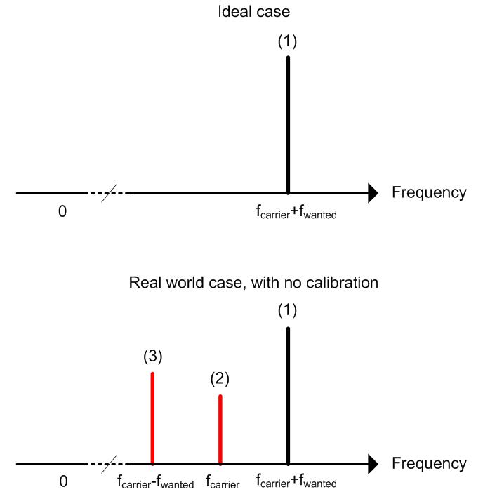
For the ideal TX case, if the continuous wave (CW) signal is up-converted to radio frequency (RF), the TX output ideal spectrum has no unwanted components, as shown in Figure 1 upper graph. In non-linear conditions, the TX output spectrum has unwanted tones as shown in Figure 1 lower graph. Descriptions of the tones are given below:
- Wanted Signal (1) – wanted TX sideband, with an offset fwanted from the carrier frequency fcarier;
- LO Leakage (2) – primarily caused by DC offsets in the TX baseband and LO leakage at the TX frequency mixing stage;
- IQ Image (3) – unwanted TX sideband, with an offset -fwanted from the carrier frequency fcarier. Primary caused by gain and phase imbalances in different IQ signal blocks.

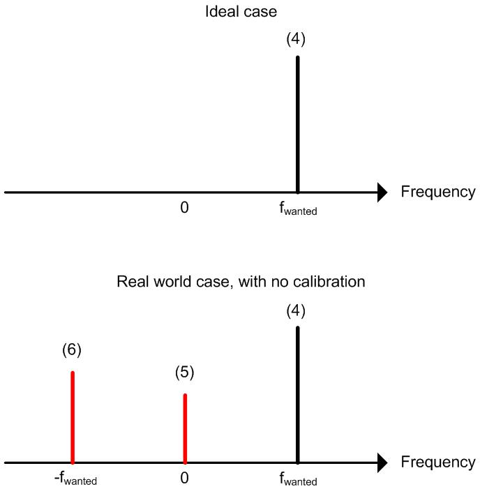
For the ideal RX case, the down-converted CW signal does not have unwanted tones at the input of the analog-digital-converter (ADC) as shown in the Figure 2 upper graph. However, under non-linear conditions the RX spectrum has unwanted signals as shown in the Figure 2 lower graph. Descriptions of the tones are given below:
- Wanted Signal (4) – wanted RX sideband, with an offset fwanted from the DC;
- DC Offset (5) – Unwanted RX DC offset. Primarily caused by DC offsets in the RX baseband and LO leakage at the RX frequency mixing stage;
- IQ Image (6) – Unwanted RX sideband, with an offset -fwanted from the DC. Primary caused by gain and phase imbalances in different quadrature (IQ) signal blocks.
Calibration procedure 1 is used to calibrate unwanted tones. The goal of the MCU program executing the calibration procedure is to find suitable LMS7002M DC offset, gain or phase correction control values for TX and RX, at which the unwanted tones are reduced to levels close to ideal cases shown in Figure 1 and Figure 2.

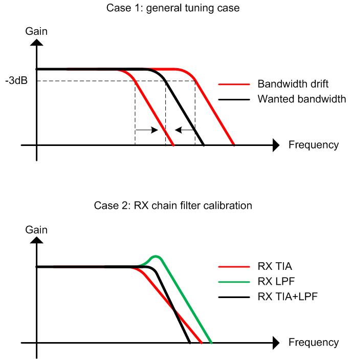
Calibration procedure 2 is used for analog filter bandwidth calibration. The procedure can be used to tune the desired filter(s) to a new bandwidth setting or to perform re-calibration on an active setup. Figure 3 shows two cases of analog filter tuning:
- Case 1 – General case. Filter -3dB bandwidth is tuned to a particular frequency or re-calibrated for a new setup;
- Case 2 – Multiple filter stage tuning. On RX side, the transpimedance amplifier (TIA) acts as a 1st order low pass filter (LPF), while the baseband LPF provides a 2nd order Chebyshev response with a 3 dB peak. Combining both filters can yield a 3rd order LPF with a tunable in-band response. Both stages need to be calibrated separately to produce the desired filter response. A similar setup is used in the TX low band stage.
The MCU program automatically selects the appropriate analog filter bandwidth calibration case in respect to the wanted bandwidth. It also handles the appropriate power down (PD) or enable (EN) controls of the involved blocks (manual setup is not needed).

General MCU calibration limitations and options
The internal LMS7002M MCU has 16384 bytes of memory, thus the size of the calibration program is limited. Furthermore, it takes time (further elaborated in Section 2) to program the MCU, hence only the main (used most frequently) calibration procedures (see Section 1.1) are stored in the MCU image. Other calibration procedures, such as PLL frequency, TX gain tuning, should be implemented as separate baseband processor routines and should be ported separately using the latest source code found on LimeSuite GitHub webpage. Thus, time for MCU image upload is reduced and the overall calibration speed is increased.
By default, MCU calibration image uses internal LMS7002M RF loopback to perform the required test signal generation procedures, hence no external components or connections are required. Nonetheless, internal RF loopback has bandwidth and signal coupling limitations. It achieves the best calibration performance up to 2GHz, but can be effectively used up to 2.7GHz (where unwanted tone suppression will decrease down to <−35dBc). External RF loopback can be used to remove the RF limitation, but this requires a modification on the board level and the use of a separate MCU image (based around the particular board). Please note, that only DC offset, LO leakage, gain and phase mismatch calibration procedures are affected by the internal/external loopback selection, while other calibration routines do not depend on board connection modifications.
Use of MCU Calibration Image
General Information
LMS7002M MCU image calibration procedures
MCU calibration image (see Section 2.1.2) has the following calibration routines that can be executed:
- Calibration of TX chain DC offset and LO leakage, phase, gain imbalances;
- Calibration of RX chain DC offset, phase, gain imbalances;
- Calibration of TX analog filter bandwidth;
- Calibration of RX analog filter bandwidth.
Other data handling procedures (for example certain variable input to the MCU) will be discussed in Section 2.2.
LMS7002M Setup Steps Needed for MCU Image Calibration Execution
LMS7002M IC must be properly set-up from the stand-point of analog and digital interface settings prior to main DC offset and LO, phase, gain calibration procedures handled by the MCU image for both TX and RX chains.
The recommended calibration/tuning priority list for TX chain is given below:
- TX and clock generator (CLKGEN) PLL frequency tuning (block order is irrelevant, baseband processor routine, see Section 1.2);
- TX analog filter bandwidth (handled by the MCU image);
- TX gain tuning (baseband processor routine, see Section 1.2);
- Settings of other TX chain controls (bias, power amplifier gain and etc.). Please note, that digital interface speed should also be configured at this or any of the earlier stages;
- TX DC offset and LO, phase gain calibration (handled by the MCU image).
The recommended calibration/tuning priority list for RX chain is given below:
- RX and clock generator (CLKGEN) PLL frequency tuning (block order is irrelevant, baseband processor routine, see Section 1.2);
- RX analog filter bandwidth (handled by the MCU image);
- Settings of other RX chain controls (bias, LNA, TIA, PGA gain and etc.). Please note, that digital interface speed should also be configured at this or any of the earlier stages;
- RX DC offset and LO, phase gain calibration (handled by the MCU image).
MCU calibration can handle a single procedure at a given time – calibrating both A and B channels or executing several calibrations procedures simultaneously at the same time is not possible. MCU calibrates only currently selected transceiver channel, which is selected by SPI 0x0020[1:0] bits. Baseband has to select channel and initiate calibration for each transceiver channel individually.
MCU Calibration Image Location
The latest MCU calibration image can always be found on LimeSuie GitHub webpage:
MCU Internal Memory Size
MCU internal memory size is 16384 bytes. It is required that all 16384 bytes have to be uploaded before the MCU becomes programmed. If program image size is less than 16384 bytes, image should be padded with zeros to meet the required size.
MCU Programming Information
Programming the MCU
- Reset MCU, write to SPI address 0x0002 = 0;
- Set one of the programming modes:
- EEPROM and SRAM, write to SPI address 0x0002 = 1;
- SRAM, write to SPI address 0x0002 = 2;
- Wait until MCU programming buffer is empty, read from SPI address 0x0003[0]:
- 0x0003[0] == 0, buffer empty;
- 0x0003[0] == 1, buffer has data;
- Write 32 bytes of program image into MCU buffer, by SPI writing to address 0x0004;
- Go to step 3. until 16384 total bytes have been written;
- Wait until MCU becomes programmed, read from SPI address 0x0003[6]:
- 0x0003[6] == 0, MCU not programmed;
- 0x0003[6] == 1, MCU programmed.
Running MCU Image Calibration Procedure
The following steps are needed to run the MCU image calibration procedure:
- SPI write 0x0006[0] = 1, switch SPI controls to MCU;
- SPI write 0x0000 = procedure ID (see Table 1);
- SPI write 0x0002[3] = 0;
- SPI write 0x0002[3] = 1;
- SPI write 0x0002[3] = 0;
- SPI read address 0x0001;
- IF 0x0001== 0xFF, MCU procedure is in progress, repeat step 6;
- IF 0x0001== 0, MCU procedure finished successfully;
- IF 0x0001== Any Other Value, MCU encountered error;
- SPI write 0x0006[0]=0, switch SPI controls back to baseband.
| Procedure ID | Calibration Procedure |
|---|---|
| 1 | TX chain calibration |
| 2 | RX chain calibration |
| 3 | Update bandwidth parameter |
| 4 | Update reference clock parameter |
| 5 | Calibrate RX analog filter |
| 6 | Calibrate TX analog filter |
| 255 | Output MCU program image ID |
Passing Parameters Into MCU Calibration Image
There are two main parameters that need to be passed to the MCU calibration program prior to executing any of the procedures mentioned in Section 2.1.1:
- Reference clock parameter;
- Bandwidth parameter.
Reference clock parameter specifies the reference clock frequency used by LMS7002M. It is passed to the MCU image with the following sequence:
- SPI write into address 0x0000 = byte0
- SPI write into address 0x0002[2] = 1
- SPI write into address 0x0002[2] = 0
- SPI write into address 0x0000 = byte1
- SPI write into address 0x0002[2] = 1
- SPI write into address 0x0002[2] = 0
- SPI write into address 0x0000 = byte2
- SPI write into address 0x0002[2] = 1
- SPI write into address 0x0002[2] = 0
- Run MCU procedure ID #4 (Update reference clock parameter, see Section 2.2.2)
Bytes have to be shifted in by triggering interrupt in MCU. Here, the reference clock parameter is passed into MCU as 3 bytes:
- byte0 – kHz LSB part;
- byte1 – kHz MSB part;
- byte2 – MHz integer.
For example, 30.72 MHz reference clock would be:
- byte0 = 208;
- byte1 = 2;
- byte2 = 30.
Valid reference clock values for different MCU calibration image procedure IDs are given in Table 2.
| Procedure ID | Calibration Procedure | Valid Reference Clock Parameter Range |
|---|---|---|
| 1 | TX chain calibration | From 10MHz to 52MHz |
| 2 | RX chain calibration | |
| 5 | Calibrate RX analog filter | |
| 6 | Calibrate TX analog filter |
Bandwidth parameter specifies the reference clock frequency used by LMS7002M. It is passed to the MCU image with the following sequence:
- SPI write into address 0x0000 = byte0
- SPI write into address 0x0002[2] = 1
- SPI write into address 0x0002[2] = 0
- SPI write into address 0x0000 = byte1
- SPI write into address 0x0002[2] = 1
- SPI write into address 0x0002[2] = 0
- SPI write into address 0x0000 = byte2
- SPI write into address 0x0002[2] = 1
- SPI write into address 0x0002[2] = 0
- Run MCU procedure ID #3 (Update bandwidth parameter, see Section 2.2.2)
Bytes have to be shifted in by triggering interrupt in MCU. Here, the reference clock parameter is passed into MCU as 3 bytes:
- byte0 – kHz LSB part;
- byte1 – kHz MSB part;
- byte2 – MHz integer.
For example, 5 MHz bandwidth would be:
- byte0 = 0;
- byte1 = 0;
- byte2 = 5.
Valid bandwidth values for different MCU calibration image procedure IDs are given in Table 3.
| Procedure ID | Calibration Procedure | Valid Bandwidth Parameter Range |
|---|---|---|
| 1 | TX chain calibration | From 2.5MHz to 120MHz |
| 2 | RX chain calibration | From 2.5MHz to 120MHz |
| 5 | Calibrate RX analog filter | From 1.4MHz to 130MHz |
| 6 | Calibrate TX analog filter | From 5MHz to 40MHz From 50MHz to 130MHz |
Configuring MCU Calibration Image
- Program MCU calibration image (see Section 2.2.1);
- Configure transceiver to working condition (refer to Section 2.1.2);
- Set chip reference clock for the MCU (optional, default 30.72MHz, see Section 2.2.3);
- Set bandwidth parameter for to be used algorithm (optional, default 5MHz, see Section 2.2.3);
- Run algorithm procedure (see Section 2.2.2);
- Wait for algorithm completion (see Section 2.2.2, step 6).
Frequently Asked Question Regarding MCU Operations
A short check-up list is given below to quickly review several important steps needed for proper MCU work:
- Is the MCU programmed?
- Is LMS7002M configured into working state prior to executing calibration procedure?
- Does the reference clock parameter passed into MCU contain the correct and actual reference clock value supplied to the LMS7002M (see Table 2)?
- Does the bandwidth parameter passed into MCU is achievable by LMS7002M (see Table 3)?
- Was the SPI control enabled for the MCU before running calibration procedure (see Question/Answer 2 below)?
Q1: MCU programming fails or program is not running.
A1: MCU requires 16384 bytes to be uploaded to become programmed. If program image size is less than 16384 bytes, image should be padded with zeros to meet the required size.
Q2: MCU can’t control LMS7002M IC.
A2: Baseband has to give over SPI controls to the MCU by SPI write 0x0006[0] = 1:
- 0x0006[0] == 0, transceiver controlled by Baseband;
- 0x0006[0] == 1, transceiver controlled by MCU.
Q3: What do the MCU error codes mean?
A3: Unfortunately because of limited MCU resources the returned error codes are not very informative, to know exact meaning of each error code, source code has to be inspected according to which procedure was used.
Q4: How much time does the calibration procedure take?
A4: Calibration duration depends on several factors:
- MCU reference clock frequency (higher frequency executes faster);
- RF sampling frequency (higher frequency reduces time needed for measurements);
- Selected procedure, each procedure has different duration.
Q5: MCU is not running procedures or is acting unpredictably.
A5: MCU relies on SPI communications with the baseband to receive parameters and initiate procedures. It might be a case that baseband SPI operations are being performed faster than the MCU can react to them.
Q6: Can MCU calibrate both A and B channels of the transceiver at the same time?
A6: No, MCU calibrates only currently selected transceiver channel, which is selected by SPI 0x0020[1:0] bits. Baseband has to select channel and initiate calibration for each transceiver channel individually.
Q7: Do I need to reprogram MCU before each procedure launch?
A7: No, it is sufficient to program MCU once after reset, and then procedures can be executed multiple times.
Example of Using API for MCU Clibration
The API function for MCU image calibration can be found here. There are 2 main functions:
- LMS_Calibrate – used for calibrations routines 1 and 2 (see Section 2.1.1);
- LMS_SetLPFBW – used for calibrations routines 3 and 4 (see Section 2.1.1).
The “LMS_Calibrate” function is described below:
LMS_Calibrate(lms_device_t *device, bool dir_tx, size_t chan, double bw, unsigned flags);
here:
- device – selects the active LMS7002M device if there is more than one present in the used design;
- dir_tx – selects either the TX or RX channel (true for TX, false for RX);
- chan – selects active channel (0 is A channel, 1 if B channel);
- bw – states the calibration bandwidth parameter in Hz.
For example:
LMS_Calibrate(lmsControl, true, 0, 5e6);
In this case TX chain, A channel LO and DC offset, gain, phase imbalances will be calibrated when a 5MHz channel bandwidth is used.
The “LMS_SetLPFBW” function is given below:
LMS_SetLPFBW(lms_device_t *device, bool dir_tx, size_t chan, float_type bandwidth);
here:
- device – selects the active LMS7002M device if there is more than one present in the used design;
- dir_tx – selects either the TX or RX channel (true for TX, false for RX);
- chan – selects active channel (0 is A channel, 1 if B channel);
- bandwidth – states the analog filter calibration bandwidth (-3dB) parameter in Hz.
A more complete example of using the MCU image calibration from API is given below:
#include "LimeSuite.h"
int main(int argc, char** argv)
{
    //Find devices
    //First we find number of devices, then allocate large enough list,  and then populate the list
    int n;
    if ((n = LMS_GetDeviceList(NULL)) < 0) 		//Pass NULL to only obtain number of devices
    	error();
    cout << "Devices found: " << n << endl;
    if (n < 1)
    	return -1;

    lms_info_str_t* list = new lms_info_str_t[n]; 	//allocate device list
    if (LMS_GetDeviceList(list) < 0) 			//Populate device list
    	error();

    for (int i = 0; i < n; i++) //print device list
    	cout << i << ": " << list[i] << endl;
    cout << endl;

    //Open the first device
    if (LMS_Open(&device, list[0], NULL))
    	error();
    delete [] list; //free device list

    //Initialize device with default configuration
    //Do not use if you want to keep existing configuration
    //Use LMS_LoadConfig(device, "/path/to/file.ini") to load config from INI
    if (LMS_Init(device) != 0)
    	error();

    //Get allowed LPF bandwidth range
    lms_range_t range;
    if (LMS_GetLPFBWRange(device,LMS_CH_RX,&range)!=0)
    	error();
    cout << "RX LPF bandwitdh range: " << range.min / 1e6 << " - " << range.max / 1e6 << " MHz\n\n";

    //Configure Receiver LPF, channel A, bandwidth 8 MHz
    if (LMS_SetLPFBW(device, LMS_CH_RX, 0, 8e6) != 0)
    	error();

    //Calibrate Receiver, channel A, using 8 MHz Tx/Rx separation
    if (LMS_Calibrate(device, LMS_CH_RX, 0, 8e6, 0) != 0)
    	error();
}